Материал: Ускоренный курс английского языка для проектировщиков сверхбольших интегральных схем. Каширский С.Н., Балашов Ю.С
Ir drop (power grid design)
Resistance in the power and ground distribution network causes IR drop. Nanometer designs are extremely susceptible to IR drop because power and ground wire resistivity increases with decreasing geometries, while the overall power supply voltage decreases. Gate delays increase non-linearly as voltage at gates decrease. The result is poor performance and increased noise susceptibility. Furthermore, gates with different voltage levels communicating with each other across the chip can propagate erroneous data, causing a malfunction. The power grid must be robust enough to prevent reliability problems from EM effects without costly over-design. In nanometer design, it is essential to understand power issues early in the design cycle, and in detail, to minimize power consumption and to address considerations such as temperature, leakage, return path, etc.
CROSSTALK AND INDUCTANCE
When signals in neighboring wires transition, the coupling capacitance between the wires can cause crosstalk. The amount of crosstalk depends on the mutual capacitance between the wires and the signal slew (i.e., the switching speed). Crosstalk causes noise problems when a transition on a fast aggressor wire causes a glitch to appear on a victim wire. The situation is more complex when simultaneous switching occurs on both wires. This situation can create crosstalk-induced delay changes which speed up or slow down signals depending on their phase relationship. Inductance between the wires can exacerbate crosstalk. Coupling capacitance and inductance effects increase with decreasing process geometries, which will make it important to account for these effects on crosstalk generation. Beyond 90 nm, it will become important to account for an increasing number of inductive effects, such as power rail “ringing” due to the simultaneous switching of multiple gates.
ELECTROMIGRATION
Electromigration occurs when the current per cross-sectional area in a wire or via is too high. In power and ground wires, a current-induced “electron wind” causes metal ions to migrate, creating voids “upwind” and metal-ion accumulation “downwind” in the form of “hillocks” and “whiskers.” Voids can also cause open circuits or increase wire resistance, which in turn increases delays and noise susceptibility. Hillocks and whiskers can cause short circuits to neighboring wires. EM is increasingly a signal wire issue as well. Wire self-heat (Joule heating) occurs when the dynamic current density is too high, resulting in EM.
DIGITAL-ANALOG INTEGRATION
Approximately 50 % of SoCs at 0.13 micron include critical analog/mixed-signal circuitry, and the percentage will increase in nanometer design. Making these sophisticated analog functions work at all, much less while sharing a
chip with a number of large digital systems, is a huge design challenge. Although the analog circuitry often accounts for only a small percent of the transistors, it accounts for 20 percent of the area, 40 percent of the design effort, and 50 percent of the respins. Nanometer digital/mixed-signal (D/MS) designs require new design approaches to optimize the chip’s overall performance and its yield. For more information regarding digital-analog convergence, see the Cadence Digital-Analog Convergence Executive Technology Brief.
POWER CONSUMPTION
Power consumption is an issue for a growing number of applications, from prolonging battery life in mobile equipment to minimizing package costs and cooling noise in stationary applications. Concerns with power consumption and the concomitant implications for temperature and reliability lead to multivoltage ICs. Other power-related issues include clocking structure design and leakage current, which increase the risk of signal integrity issues and place additional demands on ensuring electrical correctness. Since power consumption is directly related to wiring capacitance, power minimization requires careful wiring optimization and power distribution across the chip. Nanometer design tools must have the ability to cope with complex clocking schemes, multi-voltage blocks, leakage minimization, etc.
SYSTEM SIGNAL TRANSMISSION
Without effective IC packaging and timely design-in by system design teams, even the best silicon will fail in the market. High density pinouts require elaborate custom packaging, which can cost as much as the silicon itself. Ineffective chip I/O placement results can lead to silicon underutilization or even signals that are not routable. High frequency and sensitive analog/RF signals require careful, prioritized routing through the chip, package, and board. Analyzing system-level signal performance and integrity from die to die – through IC packages and across the board – is essential. Addressing system signal transmission issues is especially difficult since different design teams at different companies are often responsible for each element. For more information regarding system signal transmission, see the Cadence Silicon-Package-Board Convergence Executive Technology Brief.
MANUFACTURING RULES
Manufacturing processes using copper wiring, chemical-mechanical polishing (CMP), and subwavelength lithography lead to exceedingly complex and arcane design rules. Antenna rules, for example, require careful handling to avoid via proliferation and to minimize wire lengths. In order to minimize ramp-up time, foundries continue to change the rules until long after the introduction of a new process, and the situation is worsening with each new process node.
Nanometer routers must explicitly provide for variable width and variable spacing and must be capable of adapting to the requirements of copper wires, multiple vias, optical proximity correction (OPC), phase-shift masks (PSM), and CMP processes.
YIELD OPTIMIZATION
More than 50% of SoCs end up in high-volume applications. As processes get smaller, process variability grows. Designing for the “worst case” becomes impractically conservative, and design-centering techniques must replace the use of process corners. At nanometer levels, intra-chip variances raise a whole new level of issues. Exotic nanometer process requirements and increasingly intractable optical lithography challenges make yield management a major design issue, not simply a manufacturing issue.
5. Signal integrity closure
Class Activity
ACTIVITY 1
Introduction TEXT 1A:
Task 109. Read the passage and guess what the text is about.
For nanometer designs it is no longer sufficient to just achieve timing closure – a design must also reach signal integrity (SI) closure. SI closure implies that the design is free from SI-related functional problems and meets its timing goals while accounting for the impact of SI (see Figure 19).
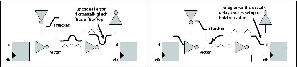
Figure 19: SI closure criteria
In the pre-nanometer design era, SI effects were either ignored or analyzed and manually repaired after achieving timing closure. This approach no longer works for nanometer designs because the number of potential SI violations exceeds what can be easily managed in a post-route analyze and repair methodology. The increase in SI problems arises from a number of technology advances including reduced feature sizes, decreases in interconnect pitch, and lower power supply voltages. With each new generation of process technology there is a dramatic increase in onchip crosstalk noise due to both the increase in the number of wires with a large percentage of coupling capacitance, as shown in Figure 20, and the accompanying rise in clock frequencies.
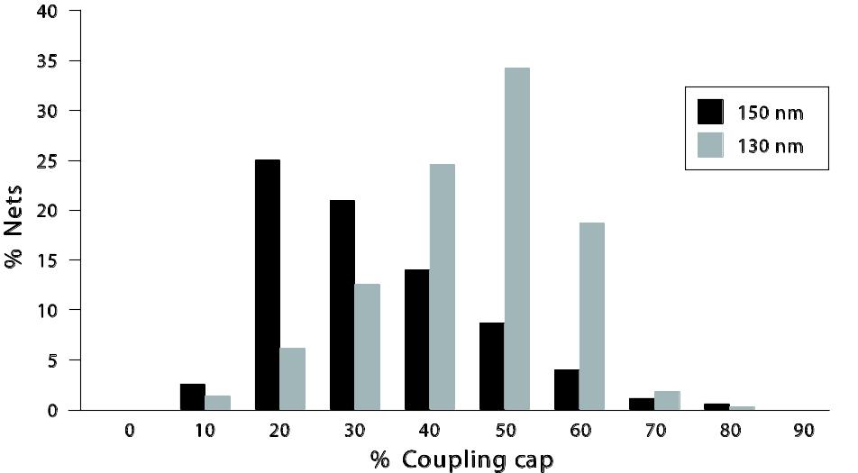
Figure 20: Percentage of nets versus coupling-cap/total-cap for 150 nm, 130 nm
For nanometer designs, SI closure must be managed simultaneously with timing closure. To achieve SI closure a design will need to undergo a number of concurrent optimization steps that prevent, analyze, and repair SI-induced problems. Each phase of the design implementation can be subject to these steps including placement, clock tree synthesis, and final detailed routing.
In applying SI optimizations a number of factors must be considered including the precision of the design data available at each stage of the design process. For example, during physical synthesis, SI optimization based on analysis of estimated routes is misleading as there is not enough wire information available to make the correct choices. Without knowing the wire track assignments and layers it is impossible to predict crosstalk effects. What is required is an implementation solution that continuously converges towards SI closure through increasing model
refinement and the appropriate amount of optimization for the given design phase. The solution must be flexible to permit different design trade-offs for different end market needs and it must be efficient without adding significant design overhead.
Task 110. Organizing your thoughts:
What does SI closure imply?
Why does the approach of the pre-nanometer design era no longer work for nanometer designs?
What does the increase in SI problems arise from?
In what way must SI closure be managed for nanometer designs?
What factors must be considered in applying SI optimizations?
Task 111. Study the sentences with the following words and word combinations:
Intellectual property (IP) blocks – блоки интеллектуальной собственности
I/Os – input/output (s) – ввод-вывод; обмен данными; устройства ввода вывода
Coupling capacitance – переходная емкость
Grounded capacitance – емкость относительно земли
Repeaters – ретрансляторы; промежуточные усилители (линии связи); линейные трансформаторы (в телефонии)
Noise-sensitive blocks – блоки чувствительные к шумам
SI closure – нарушение целостности сигналов
Routing layers – уровни трассировки
Digital cores – цифровые ядра
Analog cores – аналоговые ядра
Noise source – источник шума
Guard-ring – защитное (охранное) кольцо (транзистора в ИС)
Task 112. Read the text carefully paying attention to the italicized words and word combinations and try to understand its contents:
BASIC TEXT 1B:
SI CLOSURE METHODOLOGY
In order to efficiently achieve SI closure certain design methodology decisions should be made up front. They should be based on product schedule and market requirements. SI avoidance is the most efficient way to achieve SI closure, but it needs to be balanced against trade-offs of other design metrics such as area, performance, and power. For example, most SI problems can be avoided by spreading wires farther apart and reducing the ratio of coupling capacitance to grounded capacitance. However, if this approach is applied everywhere in the design the result is a much larger die and increased cost. For certain critical nets, such as clocks or chip-level buses, a practical solution could involve using wider wires, shielding with power and ground lines, using repeaters to break up wire lengths, using different routing layers for adjacent wires, or using 2-3X minimum spacing.
Other up-front decisions can be based around the selection of intellectual property (IP) blocks. Ideally IP blocks should neither be noise-sensitive or noise sources. This applies to all forms of IP from standard cells, memories, I/Os, and custom digital or analog cores. If an IP block is noise-sensitive or a noise source, then early decisions can be made to protect this block – such as using guard-rings, applying blockages to prevent over-the-block or near-block routing, spacing, or shielding, or even selecting an alternative implementation of the same function.
All of the SI methodology choices mentioned above can be made early in the design process. They all involve trade-offs in terms of area, performance, and engineering schedule. They can be implemented as design methodology restrictions and the implementation tools can be used to enforce the decisions in a correctly construction fashion. Creating design restrictions that minimize or eliminate certain noise sources or noise-sensitive blocks or nets prior to implementation will greatly enhance SI closure productivity.
Task 113. Fill in the gaps with the correct variant:
1. In order to efficiently achieve SI closure certain design methodology decisions should be made up...
a) back b) front c) side
2. SI avoidance is the most efficient way to achieve SI closure, but it needs to be balanced against trade-offs of the design metrics such as ….., ….. and ….. .
a) area, performance, and power
b) square, work, and energy
c) surface, operation and force
3. However, if this approach is applied everywhere in the design the result is a much larger die and ….. cost.
a) reduced b) increased c) decreased
4. For certain critical nets, such as clocks or chip-level buses, a practical solution could involve using wider wires, shielding with power and ground lines, using repeaters to break up wire lengths, using different routing layers for adjacent wires, or using ….. spacing.
a) 2-3x minimum b) 3-4x maximum c) 5-6x minimum
5. Other up-front decisions can be based around the selection of …..
a) noise-sensitive blocks
b) noise sources
c) intelligent property (IP) blocks
Task 114. Match up the words with the definition.
p |
approximation; act of approaching |
requirement |
order |
implementation |
carrying out; doing, execution (of command) |
approach |
the use of; using, something, application |
 erformance
Task 115. Look through the text again and find the following words in the sentences:
design methodology decisions
market requirements
coupling capacitance
grounded capacitance
practical solution
IP blocks
I/Os
digital or analog cores
Task 116. Organizing your thoughts:
Why should be done in order to efficiently achieve SI closure?
What is the most efficient way to achieve SI closure?
In what way can most SI problems be avoided?
What is a practical solution for certain critical nets?
What can other up-front decisions be based on?
Task 117. Sum up the text using the following plan:
Efficient ways to achieve SI closure.
Solution of most SI problems.
Other up-front decisions.
Task 118. Skim the following text and try to understand the subject-matter
of the text.
TEXT 1C:
SI PREVENTION
A number of techniques can be used to prevent SI problems during design creation. During placement for example, the placement can be optimized to avoid over-congested areas. Congested areas increase the likelihood of congested wires leading to an increase in crosstalk. Other techniques during placement include balancing slews within the design so that there are no very fast or very slow signal transitions. Very fast transitions when present on aggressors will lead to an increase in crosstalk. Weakly driven nets with slow transitions are potential crosstalk victims if there is significant coupling on these nets. Typical examples of weakly driven nets are non-timing critical signals such as resets or scan lines. These nets tend to be long and, consequently, subject to many potential aggressors. A noise glitch on a reset line can cause intermittent resetting of a chip while a noise failure on the scan line will make testing a design very problematic. Using these heuristics during placement greatly decreases the occurrence of these types of SI failures.
While SI prevention during placement will help reduce certain SI problems, the main prevention effort should come during routing. As SI is inherently a wiring problem, it has become necessary to address SI prevention as the design is being routed. Crosstalk effects, such as glitch and delay, can only effectively be measured when physical wires are available and final wire topology, layer selection, and track assignments are concrete. Since placement-based and global route-based SI prevention solutions do not have this detailed information with which to make trade-offs, they are only a partial solution. In the nanometer era, physical wire effects need to be taken into account to achieve reliable timing and SI closure during the final routing stage of the design (see Figure 21).