Материал: Ускоренный курс английского языка для проектировщиков сверхбольших интегральных схем. Каширский С.Н., Балашов Ю.С
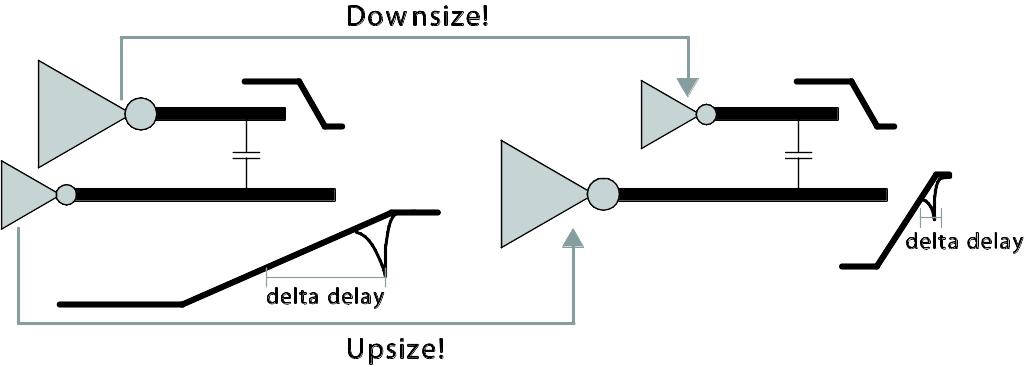
Figure 21: Slew balancing to reduce crosstalk glitch and delay effects
The key to successful SI closure during routing comes from having native on-the-fly incremental extraction, timing analysis, SI analysis, and optimization. This means that potential SI problems can be addressed as they occur. A number of prevention techniques can be employed during routing to correct SI issues:
• Wire spacing
• Net ordering
• Layer selection to reduce coupling and resistance
• Minimizing parallel wire lengths
• Shielding
• Buffer insertion
• Gate resizing (see Figure 22).
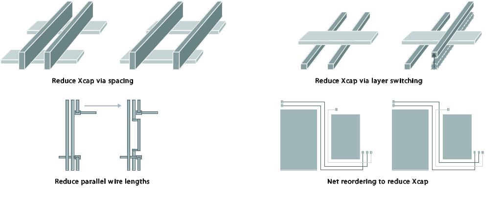
Figure 22: SI avoidance techniques during routing
Many of the above techniques require the detailed router to use a graph-based approach that supports variable width and variable spacing so that SI issues can be addressed effectively without impacting overall area. While SI analysis during routing should be accurate enough to guide the process, it must also be fast and not overburden the routing process itself. The router should also permit trade-offs in terms of meeting performance and area goals as well as preventing SI problems.
Task 119. Find sentences with the following words.
crosstalk – перекрестные помехи
noise glitch – шумовой всплеск
heuristics – эвристика
delay – задержка
graph-based approach – подход основанный на графиках, диаграммах
Task 120. Comprehension check:
What techniques can be used to prevent SI problems during design creation?
Which are typical examples of weakly driven nets?
What can a noise glitch on a reset line cause?
What is the key to successful SI closure during routing?
Enumerate a number of prevention techniques which can be employed during routing to correct SI issues.
Task 121. Match up the words with the definition.
t echnique |
resolution into simple elements |
analysis |
Resolution, solving, answer, method for solving a problem |
solution |
aims, purposes |
goals |
Mode of execution, of performance or work |
ACTIVITY 2
Task 122. Skim the following text and try to understand the subject-matter of it.
TEXT 2A:
ANALYSIS AND REPAIR
After SI-aware routing is complete, a full detailed extraction and analysis should be performed to determine if there are any remaining SI problems. This analysis should include identifying potential functional and timing problems introduced by SI. Functionality checking should involve calculating the worst-case potential crosstalk glitch that can occur on every wire and propagating that glitch to a storage element such as a latch or flip-flop to determine if it will cause a stored logic state to change.
A noise failure criterion based on latching glitches, rather than noise peak on each victim or noise rejection curves on each receiving cell, will reduce the number of potential repairs by several orders of magnitude. In a SI prevention-based flow that uses noise propagation as the failure criteria, the number of potential violations found post-route should be relatively small, typically fewer than 50 for a design with 500K instances (~2 M gates) at 250 Mhz using a 130 nm process. Consequently, repairing the remaining functional noise problems (if any) is easily achieved through automatic or even manual repair. In contrast, if the noise failure criterion is such that thousands of functional noise problems are reported, then the repair effort can be significant and may not converge.
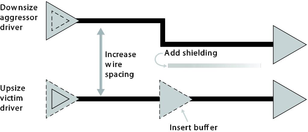
Figure 23: SI repair techniques
To repair glitch problems, a number of techniques can be used such as 1) upsizing to strengthen the victim’s driver, 2) down-sizing aggressors’ drivers, 3) buffer or repeater insertion to break down crosstalk effects into smaller constituents, 4) and spacing, shielding or re-routing wires. The key to successful convergence on repair is to find the best solution that creates the least disturbance to the existing design. For example, if re-routing a net to reduce coupling, the original timing can be maintained by restricting the length of the new route to be similar to the original route (see Figure 23).
More challenging than fixing functional violations, however, is fixing the impact SI has on timing. The additional delay changes caused by crosstalk increase the degree of difficulty for achieving timing closure. First a post-route static timing analysis of the design must be performed to determine if any new setup or hold violations have been introduced by SI. Each new failing path needs to be re-optimized. This timing repair process must endeavor to fix the failing paths with the minimum of design disturbance while identifying the optimal way to regain lost time. Fixes for timing violations can include traditional in-place optimizations as well as crosstalk reduction techniques such as those used to repair functional violations. To converge quickly on repairs, both functional and timing problems should be repaired simultaneously. As each potential repair is implemented it should be incrementally analyzed to determine if it really fixes the problem and to ensure it does not introduce a new timing or functional glitch.
After all repairs have been implemented, the design should be considered closed and ready for final verification and SI sign-off.
Task 123. Comprehension check:
What should be done after SI-aware routing is complete?
What should this analysis include?
What techniques can be used to repair glitch problems?
What is the key to successful convergence on repair?
Task 124. Fill in the gaps with the correct variant:
The analysis should include identifying potential ….. and timing problems introduced by SI.
a) functional b) external c) internal
The key to successful ….. on repair is to find the best solution that creates the least disturbance to the existing design.
a) convergence b) transition c) transplantation
The additional delay changes caused by crosstalk ….. the degree of difficulty for achieving timing closure.
a) decrease b) reduce c) increase
Each new failing path needs to be …..
a) re-elected b) re-optimized c) re-organized
After all repairs have been implemented, the design should be considered closed and ready for final ….. and SI sign-off.
a) verification b) calculation c) implementation
Task 125. Sum up the text using the following plan.
Actions to be performed, after SI-aware routing is complete.
Repairing the functional noise problems.
Techniques used to repair glitch problems.
Task 126. Skim the following passage trying to understand it and give a title to it:
TEXT 2B:
For nanometer designs timing closure is not sufficient to guarantee a working chip because it only ensures a design will operate at the desired clock frequency if it is noise free. In nanometer processes SI effects are inherent due to the high percentage of coupling capacitance versus total capacitance. Consequently, true timing closure can only be achieved when SI is taken into account. Furthermore, SI can cause functional problems. To achieve SI closure both functional and SI effects on timing must be addressed and corrected before sign-off.
Addressing SI problems after achieving timing closure is also no longer effective. The number of potential SI problems has increased substantially in the nanometer era such that SI must be tackled as the design is implemented, particularly during detailed routing. The implementation flow should strive to create an SI-clean design while still meeting other design metrics such as performance, area, and power. The flow needs to be flexible to permit trade-offs in terms of turnaround time versus creating an optimal design. Finally, the flow should support post-route repair to find and quickly fix any remaining SI-induced violations without causing any new design iterations.
An integrated SI closure approach involving prevention, analysis, and correction will significantly reduce the design cycle and, as a result, the time to market. The adoption of such an SI closure methodology will be a key determinant of success for nanometer designs.
Task 127. Comprehension check.
Why is timing closure for nanometer designs not sufficient to guarantee a working chip?
In what way can true timing closure be achieved?
What must be done to achieve SI closure?
What will be a key determinant of success for nanometer designs?
Task 128. Skim the following text trying to understand the subject-matter of it.
TEXT 2C:
NANOMETER TECHNOLOGY TRENDS
Timing sign-off is where the digital design process comes to a crunch. The goal of timing analysis is to ensure that a design will operate at the required clock frequency when it is fabricated. If the chip fails to meet its performance target, designers must implement engineering change orders–ECOs–to fix reported timing problems. Designers repeat this process until the design reaches timing closure. If designers are lucky, they reach this point within just a few iterations. But as they adopt nanometer technologies (0.18μm and below), designers find that measured silicon performance varies considerably from timing tool predictions, so additional iterations are necessary at the point where they are most costly–after fabrication.
Static timing analysis is generally the accepted timing verification method of choice for digital designers. However, most static timing tools ignore one of the key electrical side effects of nanometer processes–crosstalk induced by the simultaneous switching of neighboring wires. Crosstalk effects can distort waveforms and alter their time of flight, and so play havoc with the integrity of switching signals. If designers ignore or overestimate the impact of crosstalk on delay, designs either under perform or go through unnecessary design iterations to fix problems that don’t really exist in silicon. Either way, the net effect is a product that is late to market.
Advances in nanometer process technology aggravate timing problems because each new generation brings shrinking feature sizes, wire width, and wire spacing. The reduction in wire width means a decrease in total wire capacitance.
But it also means a dramatic increase in the fraction of wire capacitance resulting from lateral coupling. In this age of system-on-a-chip (SoC) design, die sizes have remained relatively constant as more and more functionality is crammed onto a single chip. Consequently, average wire length has remained relatively constant despite decreasing wire pitch.
The continued demand for improved performance compounds the crosstalk problem. Improved performance translates to higher clock frequencies, with much faster switching signals. As signals switch faster and faster, more noise couples onto neighboring lines. Measuring the impact of crosstalk is therefore a critical step in determining whether a design will function as expected at the required performance target.
Task 129. Comprehension check:
What is the goal of timing analysis?
What can crosstalk effects cause?
Why do advances in nanometer process technology aggravate timing problems?
What does the reduction of wire width mean?
Task 130. Skim the passage and sum up crosstalk decreasing signal delay.
TEXT 2D:
CROSSTALK IN DIGITAL DESIGNS
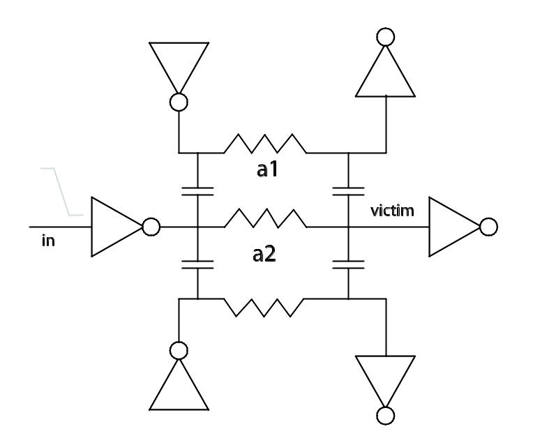
Figure 24: Victim net with two coupling aggressors
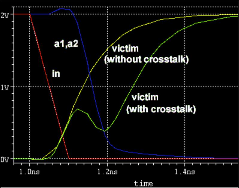
Figure 25: Crosstalk increasing signal delay
Figure 25 shows an example of the effect of crosstalk on delay for the circuit given in figure 24. The yellow waveform shows the victim signal at the receiving gate when there is no crosstalk. The green waveform shows the victim when it is attacked by an aggressor signal switching in the opposite direction. In this example the additional crosstalkinduced delay is greater than the delay of the gate without crosstalk. If the affected signal forms part of a critical maximum delay path, the extra delay due to crosstalk can cause the signal to arrive too late at a latch or a flip-flop, resulting in a setup failure.
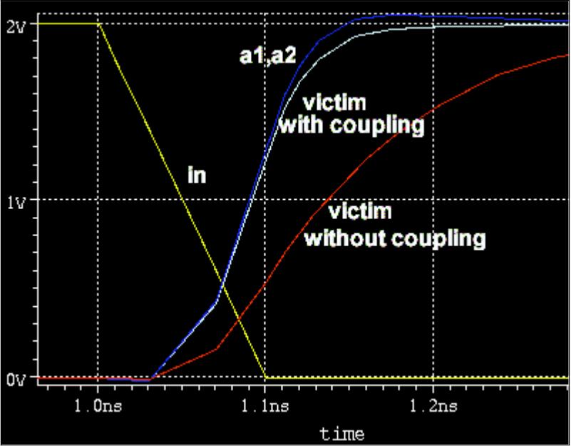
Figure 26: Crosstalk decreasing signal delay
Crosstalk can also decrease delay, as shown in figure 26. In this case, the aggressor signals (blue) switch in the same direction as the victim signal (light blue). If this occurs on a critical minimum delay path it can lead to hold violations–data arrives too early at a latch or a flip-flop. Setup failures are undesirable, but they can be removed by slowing the clock and accepting lower performance. Hold violations, however, can be fixed only by making costly silicon mask changes.
Crosstalk-induced delay effects are not limited to the nets where the attack occurs. Figure 2 shows the typical waveform shape, complete with the camel’s hump that results when an aggressor signal attacks while a victim signal transitions.
This non-monotonic waveform also impacts the delay of the following logic gate. Consequently, crosstalk effects can percolate through a circuit, and dramatically alter its timing characteristics.
Task 131. Find the sentences with the following words:
crosstalk – перекрестные помехи, перекрестные искажения
flip-flop – триггер, триггерная схема; бистабильная ячейка
latch – триггер-фиксатор; регистр-защелка
logic gate – логический элемент
Task 132. Which of the following do you think is true or false?
1. If the affected signal forms part of a critical maximum delay path, the extra delay due to crosstalk can cause the signal to arrive too early at a latch or a flip-flop, resulting in a setup failure.
2. Crosstalk can also decrease delay.
3. Setup failures are desirable, but they can be removed by slowing the clock and accepting lower performance.
4. Hold violations, however, can be fixed only by making costly germanium mask changes.
5. Crosstalk – induced delay effects are not limited to the nets where the attack occurs.
Task 133. Study the following words and word combinations:
IC – integrated circuit – интегральная схема
Power grid – электроэнергетическая система; электрическая сеть
I/O pins – контакты входа-выхода
IR drop – активное (омическое) падение напряжения; падение
напряжения на внутреннем активном сопротивлении
RC elements – элементы радиоуправления; элементы
дистанционного управления
Task 134. Skim the text and try to get its main idea.
TEXT 2 E:
POWER GRID IR DROP AND GROUND BOUNCE
C power distribution systems are designed to provide needed voltages and currents to the transistors that perform the logic functions of a chip. Based on a survey of over 206 tapeouts, targeting process technology of 0.13 micron or greater, more than 50% of tapeouts will fail if the power distribution system is not validated beforehand. At and below 0.13 micron technologies, IC designers can no longer take the risk of assuming that their VDD and VSS grids have been designed correctly, and they must perform detailed analysis to understand how robust their power distribution methodology really is.
The performance of a design’s power networks, or grid, has a direct impact on its performance. Voltage (IR) drops on VDD nets and ground bounce on VSS nets affect a design's overall timing and functionality, and if ignored, will cause silicon failure. High currents in the power grids also induce electromigration (EM) effects, where the metal lines of a power grid begin to wear out during a chip’s lifetime. These effects cause expensive field failures and major product liability issues.
While a clean power grid design should always be the goal of any design team, timing analysis should be performed with the effects of IR drop and ground bounce included once the power grid is routed – it is always possible that a designer can simply live with the amount of IR drop if it does not cause timing failure.
A complete picture of power grid robustness can only be obtained when effects such as IR drop, ground bounce, and EM are accurately computed and analyzed. These are full-chip issues that must be addressed by verification tools that have the capacity and performance required to analyze detailed representations of the chip in a reasonable amount of time. By analyzing and verifying the power grids at the full-chip level, designs can be taped-out with an increased expectation of first silicon success. In this white paper, the key issues of power grid design–IR drop, ground bounce, and EM – are described, along with the related analysis issues. Methodologies used to identify IR drop violations and potential EM violations in the power grids are also described, along with approaches that reduce the severity of these problems. Designing with these issues in mind and performing full-chip power grid verification enables designers to address what would otherwise be an intractable problem.
IR drop on a VDD grid is caused because the current demanded by the transistors or gates of a design flows from the VDD I/O pins (or bump bonds in the case of flip-chips) through the RC network of the power grid, and leads to a decreased VDD voltage at the devices. Ground bounce is a similar phenomenon, where the current flows back to the VSS pins, and the RC network causes the VSS voltage at the devices to rise. The risk of a design suffering from IR drop or ground bounce increases with shrinking process technology and with next-generation designs.