Материал: Ускоренный курс английского языка для проектировщиков сверхбольших интегральных схем. Каширский С.Н., Балашов Ю.С
With every technology shrink, the current demand per unit area of a design is increased, basically because of shrinks in the gate oxide thickness. This, combined with the fact that next-generation designs contain more transistors or gates, adds additional stress to power grid design and typically results in a power grid that contains an increasing number of parasitic RC values to be analyzed. For example, a leading-edge 90nm design containing over 10 million gates and processed with eight layers of metal could produce a VDD grid approaching 1 billion RC elements.
There are two approaches typically used for power grid analysis, static and dynamic. A static analysis solves Ohm's and Kirchoff's laws for a given power network but ignores localized switching effects on the power grid. A dynamic approach performs comprehensive dynamic circuit simulation of the power grid network, which includes localized switching effects. Both approaches have unique value and challenges.
Task 135. Speak about the two approaches typically used for power grid analysis.
Task 136. Read the following text and try to understand the subject-matter of it.
TEXT 2F:
REDUCING IR DROP
Another approach to minimizing IR drop, depicted in Figure 3, is to have a solid grid of Metal 4 and Metal 5 and use a via array to connect the two layers, effectively tying the whole grid to VDD. While this solves the problem at higher levels, it simply shifts the problem down to the lower levels of metal. What about Metal 3 and Metal 2?
Are they wide enough to handle the current levels they will sustain in terms of IR drop and EM?
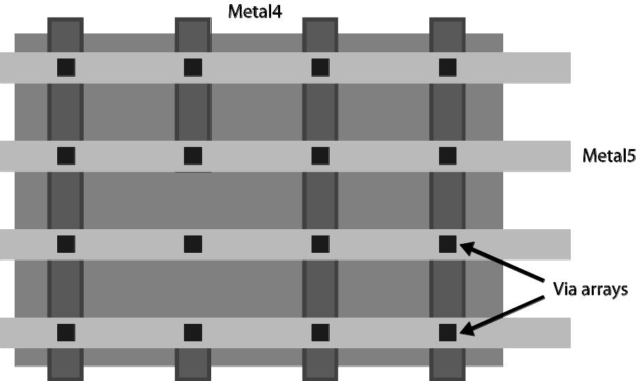
Figure 27: Vias in a mesh array methodology
Depending on the methodology, lower levels are often left floating until final assembly. Low resistance, high current paths can often be created by random placement of lower blocks. In fact, when you design the logic circuitry in the block, it is not clear where Metal 3 will tap to Metal 4, so you cannot predict the current flow. And if you cannot predict it, you must analyze it.
Part of the grid may have to be removed to route some signals, as shown in Figure 27. Which straps can be removed without introducing problems? If you arbitrarily pick one that is conducting a large amount of current, the excess current must flow in adjacent straps which may push the current density in them beyond acceptable levels. Clearly, such decisions cannot be made without determining the current levels in the straps and then picking ones that have lower current levels. The complexity of the problem requires a set of power grid analysis tools. These examples illustrate that design decisions must be made with a global perspective in mind.
IR drop is a dynamic phenomenon due primarily to simultaneous switching events in a chip such as clocks, bus drivers, and memory decoder drivers. As large drivers begin to switch, the simultaneous demand for current from the power grid stresses the grid. In a static context, IR drops are highest near the center of a design and lowest near VDD connections to the power supply. However, during dynamic operation, these simultaneous switching events can cause severe IR drops anywhere on the chip, and these are the ones that must be identified. These events, usually well known, can be triggered with typically fewer than 100 vectors.
The effect of IR drop on chip performance is significant. IR drop compromises the voltage noise margins of logic
gates, due not only to IR drops in the power grid during the rising edge of a signal, but also to the increase in voltage in the ground grid because of the same phenomenon during the falling edge. Once the noise margins drop below the budgeted amount, typically 10%, the design is not guaranteed to operate properly.
As described earlier, IR drops in the power grid can be caused by two different type of phenomena – IR and Ldi/dt.
Reducing the impact of IR drop in a power distribution system can be accomplished in several ways:
WIDEN THE POWER ROUTES
The simplest approach is to widen the lines that experience the largest voltage drops since increasing the width decreases the resistance (hence the IR drop). However, this may not always be possible due to constraints in the routing area. Via arrays should also be maximized wherever possible, since the resistance associated with a single via can have a significant impact on IR drop.
MAXIMIZE THE USE OF DECOUPLING CAPACITANCE
One effective approach is to use decoupling capacitors between power and ground, which can deliver the additional current needed by the power distribution system. These decoupling caps are usually scattered throughout the power grid, in any available space, and enable the use of the static approach to power grid analysis. Ldi/dt effects can be mitigated by placing large capacitances near the pins.
STAGGER THE SWITCHING
Since IR drop is due primarily to simultaneous switching events, another (more difficult) approach is to stagger the gates that are switching together such that they switch at slightly different times – at least enough to keep the problem within the noise budget. Alternatively, you could reduce the buffer size, but this may not be possible if the design fails to meet performance requirements with smaller devices. Device switching can be staggered to reduce the peak demands of current by introducing delays on the signals driving the gates.
MAXIMIZE THE POWER I/O PINS
A more aggressive solution is to use a ball-grid array, sometimes called solder bumps or C4 bumps, where the power supply connections can be at various points within the chip. This expensive solution requires placing many C4 bumps across the chip to minimize the worst-case IR drop in any location. This solution tends to push EM problems to lower levels of metal that are usually narrower. Also, this solution cannot be used in sensitive areas such as memories and dynamic logic because C4 bumps generate alpha particles that may cause logic value upsets in the sensitive nodes.
Nevertheless, when used appropriately, C4 bumps can reduce IR drop. The key to design is proper placement of the C4 connections, which can only be done effectively with full-chip analysis
Task 137. Give a short summary of the text with the help of fig.27:
ACTIVITY 3
Vocabulary work and situations.
Task 138. Guess the meanings of the following words and word combinations:
Phenomena
Distribution
Effective
Solution
Sensitive areas
Alpha particles
Task 139. Try to recognize the words in the following sentences and translate them into Russian.
As described earlier, IR drops in the power grid can be caused by two different types of phenomena – IR and Ldi/dt.
Reducing the impact of IR drop in a power distribution system can be accomplished in several ways.
One effective approach is to use decoupling capacitors between power and ground which can deliver the additional current needed by the power distribution system.
A more aggressive solution is to use a ball-grid array, sometimes called solder bumps or C4 bumps, where the power supply connections can be at various points within the chip.
Also this solution cannot be used in sensitive areas such as memories and dynamic logic because C4 bumps generate.
Task 140. Define the meaning of each word with the help of an English-English dictionary. The first example is given to you.
System – complex whole, set of connected things, or parts, organized body of material or immaterial things.
Approach –
Resistance –
Solution –
Metal –
Analysis –
Device –
Array –
Task 141. Match up the words with their definitions:
G |
Method, way of doing or performing something |
technique |
Invention, thing adapted for a purpose |
power |
Purpose, aim |
device |
Vigour, energy |
 oal
oal
SITUATIONS:
Discuss the ways of reducing IR drops.
Speak about the approach to minimizing IR drop depicted in Fig.27
Discuss the effect of IR drop on chip performance.
OUTCLASS ACTIVITY
Task 142. Read the text and pay attention to the concepts on which most static approaches are based.
STATIC POWER GRID ANALYSIS
The static power grid analysis approach was created to provide comprehensive coverage without the requirement of extensive circuit simulations. Typically, most static approaches are based on similar concepts:
1. The parasitic resistance of the power grid is extracted
2. A resistor matrix of the power grid is built
3. An average current for each transistor or gate connected to the power grid is calculated
4. The average currents are distributed around the resistance matrix, based on the physical location of the transistor
or gate
5. At every VDD I/O pin, a source of VDD is applied to the matrix
6. A static matrix solve is then used to calculate the currents and IR drops throughout the resistance matrix
A static approach approximates the effects of dynamic switching on the power grid by making the assumption that de-coupling capacitances between VDD and VSS smooth out the dynamic peaks of IR drop or ground bounce.
The main value of the static approach is its simplicity and comprehensive coverage. Since only parasitic resistance of the power grid is required the extraction task is minimized, and since every transistor or gate provides an average loading to the power grid the solution provides comprehensive coverage of the power grid.
The main challenge of the static approach is accuracy. Local dynamic effects are not accounted for, neither are package inductance effects (Ldi/dt), both of which may result in optimistic IR drop or ground bounce results if there is insufficient de-coupling capacitance on the power grid.
Task 143. Read the text again and enumerate the concepts.
Task 144. Read the text and get information about reducing electro–migration problems.
DYNAMIC POWER GRID ANALYSIS
A dynamic power grid analysis requires that both resistance and capacitance of the power grid are extracted, and that a dynamic circuit simulation of the resistant RC matrix is completed. Typically, the steps to complete a dynamic power grid analysis are:
1. The parasitic resistance and capacitance of the power grid is extracted
2. The parasitic resistance and capacitance of the signal nets is extracted
3. The design netlist is extracted
4. A circuit netlist is created from the extracted parasitics and netlists
5. A circuit simulation is executed, based on a suite of simulation vectors, which simulates the transistors or gates dynamically switching and the effect of this switching on the power grid. The main value of the dynamic approach is its accuracy. Since the results are based on circuit simulation, the IR drop and ground bounce results can be extremely accurate and take into account localized dynamic and package inductance effects.
The challenges of the dynamic approach are significant.
• The parasitic extraction demands are high because you need to extract resistance and capacitance for the power grids and (as a minimum) the capacitance for the signal nets.
• The circuit simulation can contain a huge number of elements to be simulated, which strains the capacity of the circuit simulation engine.
• The vector set that is used to stimulate the simulation plays a dominant role in determining the quality of the output, if a comprehensive suite of vectors is not used, then the results will be questionable because sections of the power grid may not have been simulated.
• Finally, given the number of elements associated with a single power grid, a power grid analysis solution based on comprehensive dynamic simulation will not easily scale as design sizes continue to grow.
Many power grid analysis solutions that promote a dynamic approach must often resort to RC reduction techniques to manage the size of the data to be simulated; however, this directly conflicts with the main value of the dynamic approach, the accuracy of the results. RC reduction of the power grid can cause inaccuracies to creep into the analysis, and can hide real EM problems.
SUPPLEMENTARIES
The following table shows results from a number of 130 nm customer designs that have been implemented using the Cadence® SI closure flow that is an integral part of SoC Encounter™. In each case the design has been successfully fabricated without any SI-related problems. In addition, all of the designs operated at the desired clock frequency (see Figure 28).
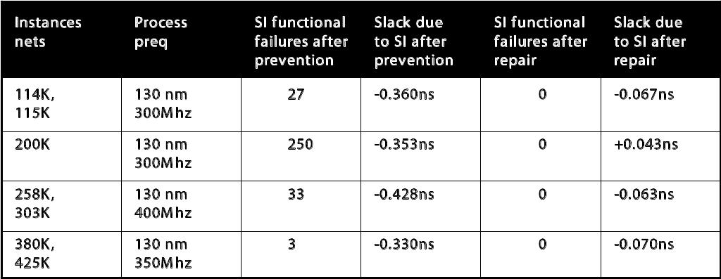
Figure 28: Results of using SI closure on real 130 nm designs