Материал: Ускоренный курс английского языка для проектировщиков сверхбольших интегральных схем. Каширский С.Н., Балашов Ю.С
High database performance enables many tools to operate directly off the database, saving application development time. While some tools will use their own proprietary data structures for runtime efficiency, the persistent repository will remain the centralized database. If the database also has an appropriate extensibility model, fewer and fewer applications will duplicate structures, such as the netlist, that already exist in the database.
It is impossible to predict all future design information requirements, so nanometer databases should support the creation of new object types, the addition of attributes to existing objects, and the definition of new relationships among objects – all with native speed and efficiency. Such extensions must be lightweight, space-efficient, timeefficient, and optimized for the particular data type.
With appropriate extensibility, application developers – including in-house and third-party tool developer – can write efficient algorithms to manipulate and analyze the data they need precisely at full speed. Extensions should be available permanently to enable other tools to use them, or temporarily to serve as a coherent high-performance cache. In-memory coherence makes it possible to write tools built from cooperating components that are incremental in nature, to use lazy evaluation techniques, and to provide application-level toolkits that allow rapid new tool evolution and construction.
Nanometer databases should be open, which includes having an open application programming interface (API), open source code, and a community-based oversight committee. Openness is not a technical requirement per se, but it directly facilitates a technically superior implementation that advances rapidly. It also mitigates design team risk by enabling native third-party and in-house application development.
Task 102. Give a short summary of the text with the help of fig.15.
ACTIVITY 3
Vocabulary work and situations.
Task 103. Guess the meaning of the following words and word combination.
writing delay
neighboring wires
IR drop
routing
logic gates
silicon virtual prototype
nanometr routing requirements
delay calculation
Task 104. Try to recognize these words in the following sentences and translate them into Russian.
Writing delay accounts for the vast majority of overall delay.
“Sign off” timing analysis tools miss numerous SI and IR drop based degradations that are comparable in magnitude to the nominal timing and much more difficult to predict.
Delay is a function of wire loading and wire drive.
Resistance in the power and ground wire networks creates IR drop.
Traditional IC implementation approaches are linear in that designs move sequentially through a series of stages – RTL, gates, power planning, placement, clock tree design, routing, and physical analysis.
Task 105. Define the meaning of the given words using English-English dictionary. The first example in given to you.
Solution is an answer to, or way to dealing with a problem.
gate
routing
placement
delay
Task 106. Match up the words with the definition.
d |
the controlling electrode of a field – effect transistor |
requirements |
the property of a system that enables it to store electrostatic charge |
capacitance |
that which is required |
gate |
a time interval or a voltage bias |
 elay
elay
SITUATIONS:
With the help of fig.1 try to explain wire and gate delay in Al and Cu.
Comment upon crosstalk in the design of wires.
Share your opinion on the need for a new design strategies.
Discuss the role of massive routing capacity and performance.
OUTCLASS ACTIVITY
Task 107. Read the text carefully and pay attention to total delay in design performance.
DESIGN PERFORMANCE
The total delay associated with a net or path is governed by a simple equation that includes device delays, device loads, and slew rates. The delays caused by device loading are known as interconnect delays. The equation could be represented as:
Total delay = device delay + interconnect delay + slew rate (see Figure 16)
When process geometries were greater than one micron, the performance of a design could be accurately predicted by analyzing device delays and approximating (or in some cases, ignoring) the interconnect delays and slew rates.
Device loads were typically treated as a lumped capacitance, an approximation enabled by the fact that device delays dominated the equation. Slew rates were also typically ignored for the same reason.
As processes shrank below one micron, these approximations became more and more inaccurate. With the total delay decreasing, slew could no longer be ignored, since it affected a more significant percentage of the total delay. For the same reason, device loads could no longer be accurately represented by a simple capacitance, so the lumped RC model was introduced. Despite these relatively minor changes, device delays still dominated the total delay equation.
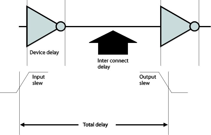
Figure 16: Total delay is equal to device delay plus interconnect delay and slew rate
An interesting phenomenon occurred as the process geometries shrank below 0.5 microns. Somewhere in the 0.5-0.35 micron process size, the interconnect delay caused by device loading became equal to the device delay.
This event, while not perceived to be a dramatic change, emphasized the effects of DSM by changing the basic paradigm of design: gate delay no longer dominated interconnect delay. Original approximations based on this paradigm failed, and interconnect delays could no longer be treated as second order effects. Since interconnect delays began to play a major role in determining total delay, the distributed RC model was introduced to improve the accuracy of interconnect modeling.
Shrinking the process technology past DSM and down to ultra-deep submicron (less than 0.25 micron) will continue the delay trends and introduce some additional concerns. Total delay will continue to decrease, interconnect delay will continue to increase (eventually dominating device delay), and slew will continue to play an important role in determining total delay. Also, increased coupling capacitance between adjacent interconnect wires will increase delay times and cause hard failures due to noise injection. Voltage drop and ground bounce in poorly designed power rails will also impact delays due to weakened driver strengths. For high performance designs, inductance
will start to play a role in interconnect delays, and the delay model will transition from a distributed RC model to a distributed RLC model.
Task 108. Read the text and explain the interconnect verification in design.
Interconnect verification
With interconnect delay continuing to increase in importance, more effort must be spent in verifying interconnect, which involves the initial extraction of the interconnect parasitics followed by different types of interconnect analysis. This can be expressed in a simple equation:
Interconnect verification = extraction analysis
The amount of interconnect verification performed on a design is dependent on the target process technology, frequency, and the design itself. Designs targeted to a non-DSM process technology will not experience the same severity of interconnect-related problems as a design targeted to a UDSM technology. Similarly, high-performance designs such as today's microprocessors and microcontrollers will typically require significantly more interconnect verification than more conservative designs running at much slower clock frequencies. Figure 17 provides guidelines on when interconnect verification may be required.
Interconnect verification is both frequency- and process-dependent; however, as process technologies continue to shrink, interconnect verification becomes more of a necessity.
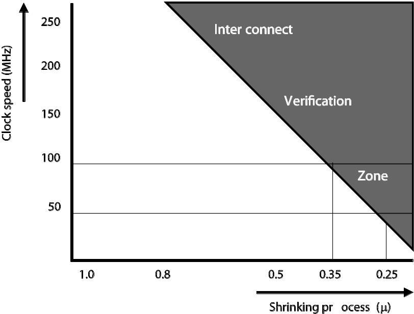
Figure 17: The need for interconnect verification depends on clock speed and process size
What is the risk of not performing interconnect verification? For a conservative design methodology, over-design could prevent most serious performance problems, but even over-design does not guarantee problem-free tape-outs.
For example, one design team took a conservative design approach to avoid having to manage the complexities of additional clock verification. To ensure good clock performance, they over-sized the clock buffers. However, the increased buffer sizes caused voltage (IR) drops in the power grid that actually caused the clock performance to be worse.
For an aggressive design methodology, the chances of taping out a design that performs to its intended specification without performing interconnect verification are severely diminished. An example of this was a design team where, using a more aggressive design methodology, it eventually took 100 engineers hand modeling the layout to find a coupled capacitance that slowed down a critical net.
SUPLEMENTARIES
FULL-CHIP VS. CRITICAL NET EXTRACTION
Two design methodology approaches are used for parasitic extraction. The first assumes the full-chip netlist can be divided into two groups, critical nets and non-critical nets. Once divided, each group is treated differently, such that the critical nets are extracted with high accuracy and the non-critical nets are extracted with low accuracy.
The reasoning behind this approach is that not all nets require accurate extraction, and so there is a runtime vs.
accuracy tradeoff made for the non-critical nets. The alternative approach assumes that the capacitance extracted from any net could be associated with a critical net, and therefore, all capacitance should be extracted with high accuracy. This is the most predictable approach for DSM and UDSM technology. The lateral and fringe components of capacitance clearly dominate below 0.25 micron, and coupling capacitance is dominated by these components. The ratio of coupled to non-coupled capacitance continues to increase as the process technology shrinks.
The danger with the first approach is that there is no guarantee that all critical nets are identified. The filtering mechanism used to divide the full-chip netlist must account for all factors that could determine criticality, including driver size, distributed RC load, coupling between nets, and signal timing. While it may be possible to identify critical nets based on the first two criteria, it is extremely difficult, if not impossible, to pre-determine criticality based on the last two.
Consider the following example: Three nets, pre-determined to be non-critical (based on driver size/loading criteria), are tightly coupled to each other because their routes are adjacent. The central net has a large driver and large capacitive load, which causes the adjacent nets to become critical due to high coupling capacitance (see Figure 18).
Since all of these nets were pre-determined to be non-critical, all of the associated capacitances are extracted with gross accuracy, despite the fact that high coupling capacitances A and B have caused two of the nets to become critical.
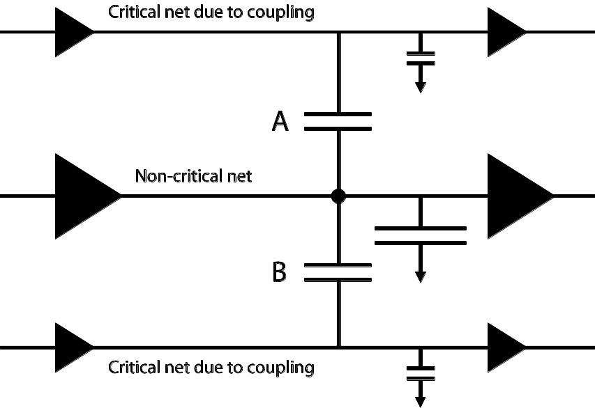
Figure 18: All capacitance is extracted with gross accuracy, even for critically coupled nets
Below are descriptions of 10 top technical issues associated with nanometer design.
-
#
Issue
Wire related
1
2
3
4
5
6
7
8
9
10
Design size and complexity
Timing based on SI and IR
IR drop (power grid design)
Crosstalk and inductance
Electromigration
Digital-analog integration
Power consumption
System signal transmission
Manufacturing rules
Yield optimization
Yes, if hierarchical
Yes
Yes
Yes
Yes
Somewhat
Somewhat
Yes
Yes
Yes
DESIGN SIZE AND COMPLEXITY
At 0.18 micron, there are designs with over 250 million transistors. Nanometer designs will support multiple-billion transistors within the next few years with no corresponding relaxation of time-to-market demands. Implementing these designs will require nine or more layers of metal, multiple metal pitches, via densities measured in millions per square centimeter, and pervasive use of flip-chip packaging to distribute thousands of I/O pins. These advances create three related issues designers must address – capacity and performance; early, accurate analysis; and hierarchy to manage complexity. A nanometer design environment must have the capacity and performance to handle these huge chips while imposing as few methodology restrictions as possible.
TIMING BASED ON SIGNAL INTEGRITY AND IR DROP
As described throughout this paper, timing analysis in nanometer designs that does not include signal integrity (SI) and IR drop effects is essentially meaningless. At 0.13 micron, “sign-off” timing analysis tools fail to catch numerous SI and IR drop based degradations that are often comparable in magnitude to the nominal timing and much more difficult to predict. Timing nanometer designs accurately requires realistic wires, advanced interconnect modeling techniques, and sophisticated physical analysis.