Материал: Ускоренный курс английского языка для проектировщиков сверхбольших интегральных схем. Каширский С.Н., Балашов Ю.С
To ensure that electromigration failure does not occur in the field, we need to limit the current density such that electromigration failure will not become significant until long after the projected useful lifetime of the circuit.
This is a function of not only the current density in the metal lines and contacts, which may behave differently, but also of temperature and often process variations.
Task 56. Comprehension check.
Explain with the help of the equation the Black`s law.
When does electromigration failure take place?
Task 57. Skim the following text trying to understand the subject-matter of it.
TEXT 2C:
EFFECT OF TEMPERATURE ON CURRENT DENSITY LIMITS
The major effect of temperature on electromigration is in the diffusion coefficient. Diffusion is a thermally activated process characterized by the Arrhenius relation and it possesses an activation energy. The activation energy for self diffusion depends strongly on the diffusion mechanism. Diffusion can proceed through the lattice, or grain boundaries, and along interfaces or the surface. The lattice is the most difficult path with the highest activation energy (for Al DHlattice is about 1.4 eV), followed by the grain boundary (for Al, DHgrain boundary is about 0.6 eV ) and then the surface. In Al, the surface is generally not available due to the presence of a coherent oxide film. Interfacial diffusion activation energies differ for every interface and can be either greater or less than that for grain boundary diffusion. Adding alloying elements generally has the paradoxical effect of decreasing the lattice and increasing the grain boundary activation energies. The effect on interfaces is unclear.
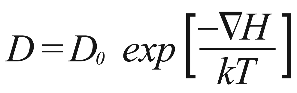
Where D0 is a pre-exponential factor that depends on the diffusion mechanism and DH is the activation energy, also dependent on the diffusion mechanism.
Equation 3 shows that electromigration is very sensitive to temperature. For Al, generally a change in temperature of 20 degrees can double the rate of electromigration. Therefore, the current permitted in a thin film conductor is a function of temperature. The higher the temperature, the less current can be permitted and still remain safe from electromigration failure.
Just how much current can be permitted and still maintain reliability as the temperature is changed will depend on whether you have nucleation or growth dominated failure and what the dominant diffusion mechanism is. If we have growth-dominated diffusion and we increase the temperature such that we double the diffusion coefficient (approximately 20 degrees for Al alloys and grain boundary diffusion), we must reduce the current density by half.
Conversely, if we want to increase the current density by a factor of two, we must ensure that the temperature is at least 20 degrees cooler. If failure is nucleation dominated, an approximate 30 % reduction in current is needed for a similar temperature increase to maintain equal reliability.
Whether failure is nucleation or growth dominated is a matter of the process used to deposit the metal and the overlying dielectric. Almost everything that happens consists of an initiation followed by a continuation.
Electromigration is no exception. First the damage must be initiated, a void nucleated or an extrusion formed, then the damage proceeds, such as void growth or continuing the extrusion, until failure occurs. Sometimes nucleation is slow and takes a long time and growth is fast. When this happens we have nucleation dominated failure. Sometimes we have the converse, and the nucleation is either very short or non-existent, and we then have growth-dominated failure. Electromigration exhibits both types of behavior.
Task 58. Comprehension check:
What is the diffusion coefficient?
What does activation energy depend upon?
What does equation 3 illustrate?
Task 59. Skim the passage and find out how the thermal heating is formed.
TEXT 2D:
RMS CURRENT AND TEMPERATURE GRADIENTS
When current is passed through a conductor, the interaction of the electrons with the lattice produces a thermal energy equal to the product of the square of the current and the resistance. This is called Joule heating. Metal lines will heat up whenever current is passed through them. If the current is low, the heat is effectively conducted away, but there must be some temperature increase even if it is not detectable. If the current density approaches 106 A/cm2, Joule heating can produce enough energy to make the conductor lines heat up appreciably. At first this does not appear to be a problem, since current densities are almost always lower than this due to limitations induced by electromigration. However, one must realize that Joule heating is caused by root mean square (RMS) current and not by the average current, as is electromigration. For a narrow pulse, the RMS current can be much higher than the average current. The average current can be well within any guidelines that may be set for electromigration considerations, yet significant Joule heating can result. This can be more prevalent on upper level metallization, where heat must be conducted through several layers of interlevel dielectric, which is a poor thermal conductor.
The problem with Joule heating is not the modest temperature increase, but the temperature gradients that result.
Typically, at the current densities found in modern circuitry, temperature increases would range between a few and a few tens of degrees Celsius. This produces temperature profiles that decay within a few microns, so that temperature gradients of 104 to 105 degrees Celsius/cm will be found. Since electromigration is thermally activated, the temperature gradients produce flux divergences that approach that found at absolute divergences such as at contacts or at microstructural features.
RMS current density must then be limited to about 2 x10⁶ A/cm2 for lower level lines and about half that for upper level lines. Unfortunately, the reliability of metal lines in the presence of temperature gradients cannot be accurately estimated.
Temperature gradients can vary tremendously throughout a real structure, depending on subtleties of the geometry and on the use of the underlying silicon devices. The only way to deal with these issues is to take a conservative approach and forbid temperature gradients by limiting the RMS current density to the levels suggested above.
Task 60. Find the sentences with the following words:
thermal energy – тепловая энергия
joile heating – тепловая энергия
RMS Root mean equal – среднеквадратичное значение
average current – средний ток
divergence – различие
Task 61. Which of the following do you think is true or false?
1. Thermal heating passes through the conductor.
2. Joule heating does not pass electric current.
3. Temperature gradients produce flux divergences found at microstructure.
Task 62. Study the following words and word combinations in the following sentences:
Joule heating – джоулевое тепло
Temperature gradients – температурные градиенты
RMS current – среднеквадратичный ток
Task 63. Skim the text and try to get its main idea.
TEXT 2 E:
MICROSTRUCTURE AND ELECTROMIGRATION LINE WIDTH EFFECTS
Electromigration is a form of mass diffusion, where the driving force is provided by the electron flow. Therefore, things that affect diffusion will affect electromigration. Metals are composed of atomic crystals where atoms are lined up very nearly perfectly in only a few allowable configurations. The size of these crystals (“grains”) is finite.
Where the grains meet, they form a region of disorder (“grain boundary”), and provide a pathway for easy diffusion as compared to the nearly perfect metal lattices.
In the early days of ICs, the thin film conductors used in manufacturing were relatively wide, fine grained, and composed of many grains. These were referred to as polycrystalline. The grain size was about the thickness of the film, generally about one micron. Across the width of a typical conductor several microns wide, many grain boundary pathways were available to accommodate the electromigrating atoms. It came as no surprise that electromigration failure was inversely proportional to the grain size of the films: the more grain boundaries present, the more atoms that can be transported along them, and the earlier the failure time.
As line widths became smaller, the grain size of the metal films became larger. Conductor lines became comparable in width to the grain size and took on a “bamboo” like appearance where most of the grains spanned the line width, providing no continuous grain boundary pathway in the direction of the current flow. When this occurred, a peculiar effect was found: failure times were strongly dependent on line width. Narrow lines at the same current density became substantially more reliable than wider lines, as long as the grain size was uniform.
The reason for this behavior was not hard to figure out. The lack of easy grain boundary pathways meant that the atoms had to take more arduous paths such as the lattice or various interfaces in their journeys. The activation energy for failure was found to be a function of line width, since the diffusion process changed. What became even more interesting and important to reliability engineers was that the precise arrangement and orientation of the grains had a large effect on the lifetime of the conductor. In fact, as the ratio of grain size to line width increased, the reliability became poorer before it got better, and then got worse again as lines entered submicron widths.
Today, we understand this behavior and can predict the reliability from test data, grain structure, and particulars of the metal deposition process. New effects, due to the presence of refractory shunt layers and W plugs, have surfaced and have also been explained well enough that they can be tamed. However, a fundamental understanding of the process of solid state diffusion and what affects it are essential in interpreting test results. For this reason, conservative default values for parameters used in relating electromigration test data to real circuits should be employed until careful testing and data interpretation justify a change.
The choice of test structures and test conditions are of critical importance in extracting meaningful parameters to be used in interpreting the test data as it relates to actual chip performance. The wrong test or the wrong test structure can produce fatal results. The test structure must be designed to reflect the process and usually a single structure cannot.
Task 64. Give explantation of electromigration in the electron flow.
Task 65. Read the following text and try to understand the subject-matter of it.
TEXT 2F:
PHYSICS OF ELECTROMIGRATION
Electromigration is due to the momentum exchange between conducting electrons and diffusing metal atoms. Simply stated, perhaps, but how does it happen?
In a perfect lattice, there is no resistance. Electrons move about in a periodic potential with no other interaction with the metal atoms. This may sound like superconductivity, but it isn’t. The problem here is that a perfect lattice cannot exist above absolute zero due to missing atoms (“vacancies”), impurities, boundaries between crystals of different orientation (“grain boundaries”), and regions of imperfection (“dislocations”). Perhaps even more important, at any temperature above 0o K, atomic vibrations occur. These vibrations (“phonons”) put a metal atom out its of perfect position about 1013 times each second and disturb the periodic potential, causing electron scattering.
The scattering event makes the electron change direction; any change in direction is accompanied by an acceleration; and for every acceleration there is a force. After many collisions (another word for the scattering event), the force averages out in the direction of electron flow.
The force due to collisions of electrons to metal atoms is called the momentum exchange. In electromigration, momentum is exchanged between the electrons and the metal atoms and a change in momentum with time is called a force. To provide sufficient momentum exchange to cause measurable effects, many electrons must be available to collide with the atoms. This can only happen in a metal. In metals, many electrons are easily accelerated in an electric field.
Semiconductors have far fewer electrons and in a true semiconductor, electromigration does not exist because there just aren’t enough charge carriers. However, electromigration can occur in semiconductor-like materials, such as silicon, when they are so heavily doped that they act as if they were metals. At dopant levels of around 1%, electromigration has been observed in polycrystalline silicon, but then the temperature coefficient of resistance (TCR) is positive. A positive TCR is probably the best definition of a metal.
The size of the momentum exchange will be proportional to the distortion in the lattice at any given point. This distortion is greatest when there is a vacancy nearby, or in the region of a grain boundary. This is also where diffusion occurs. Vacancies or grain boundaries must be present for metal atoms to move from their fixed positions in the crystal lattice (“diffuse”). You can’t have two things in the same place at the same time, so for an atom to move from site A to site B, site B must be vacant. In grain boundaries the problem is less well defined, but the concept still applies. However, a boundary is a region of distortion and open space, and the diffusion of atoms can be accommodated in these regions rather easily as compared to the lattice. This creates a fortuitous situation where the greatest momentum exchange occurs only at the sites where it is possible for atoms to move.
For the design engineer, electromigration physics can be simply stated. Electrons flow through a metal film and collide with metal atoms. The collisions produce a force on the metal atoms in the direction of electron flow (for n-type materials, opposite for p-type materials). Electromigration is only significant at high current densities and only in metals. The magnitude of the electromigration force is proportional to the current density.
Task 66. Give a short summary of the text paying attention to the formation of line width effect in electromigration.
ACTIVITY 3
Vocabulary work and situations.
Task 67. Guess the meaning of the following words and word combinations:
joule heating
RMS current density
reliability budgeting
root tools
temperature gradient
Task 68. Try to recognize the words in the following sentences and translate them into Russian.
To manage EM, designers first need to understand …… .
A mean time to failure (MTTF) ….. .
Power grid EM issues can be solved with ….. .
Which electrons flow through wires on a chip, they collide …. .
EM is a thermally activated phenomenon ….. .
Electromigration is due to take momentum exchange between conducting electrons ….. .
Task 69. Define the meaning of such words using English-English dictionary. The first example in given to you.
Electromigration –
to manage –
grid –
Task 70. Match up the words with the definition.
p |
any outburst of violent weather |
to dissipate |
energy, stress |
real |
existing in reality, in fact |
storm |
to go away or cause to away |
 ower
ower
SITUATIONS:
Discuss tools which IC designers need for EM.
Comment upon the role of routing.
Figure out the problem of Joule heating and explain the current density.
OUTCLASS ACTIVITY
Task 71. Read the text and pay attention to the electromigration behavior force.
GROWTH – DOMINATED FAILURE
If there is a redundant shunt layer, the initial rapid growth of the void will not produce an open circuit. The shunt layer, usually of a refractory material such as W or TiN, can conduct electricity even if a void exists in the primary Al conductor. These metals can withstand extremely high current densities at high temperatures for very long times.
If failure is defined as an open circuit, they don’t fail. However, for most realistic situations, an open circuit is not a realistic definition of failure. Since a resistance change of about 10 % in global wiring can produce timing errors, the 10 % increase has often been chosen as a failure criterion.
Using a percentage increase as a failure criterion during a test has some problems. The actual damage that causes a failure will be a function of the precise geometry of the test structure and the initial resistance. This is unsatisfying for evaluating real circuits that don’t look like test structures. It is recommended, therefore, that failure criteria be based on an absolute change in resistance, the maximum that a particular circuit can withstand before problems arise.
It is necessary to use test structures that can measure a resistance change without geometric effects, such as the Blech Length to affect the data. In the 1970s Ilan Blech of the Technion in Israel performed one of the most important series of experiments in the history of electromigration science and technology. In these experiments he had created a test structure that consisted of islands of gold (Au) deposited onto a refractory underlay. When current was passed through these samples, the upstream side of the islands moved in the direction of electron flow and the downstream edge stayed stationary. If the island was long enough, extrusions formed on the downstream edge, but if the island was short enough, electromigration essentially stopped. Electromigration also stopped when the longer islands shrunk to a critical level. He discovered that there is a critical product of the current density and the length of the island, below which electromigration ceases. This is the origin of the “Blech Length.” For any given current density, there is a length below which electromigration will not occur.