Материал: Ускоренный курс английского языка для проектировщиков сверхбольших интегральных схем. Каширский С.Н., Балашов Ю.С
3. What is electromigration?
Class Activity
ACTIVITY 1
Introduction TEXT 1A:
Task 38. Read the passage and guess what the text is about.
Electromigration (EM), the mass transport of a metal due to the momentum transfer between conducting electrons and diffusing metal atoms, exists wherever current flows through metal wires. Discovered more than 100 years ago, EM first showed up in ICs as early as 1966 and has been a persistent problem since the early days of IC manufacturing.
When electrons flow through wires on a chip, they collide with metal atoms, producing a force on the atoms that causes the wires to break over the chip’s lifetime. When early ICs were returned from the field and examined under a microscope, very fine “cracks” in the wires were found. The immediate fix was simple: make the metal wires thicker. Making wires thicker was easy when they were 10 microns wide, but, due to the difference in aspect ratio, it’s not easy with today’s 130 nanometer and 90 nanometer technologies.
The conditions necessary for EM to be a significant problem continue to bear down on us with increasing speed and ferocity: high current densities, long narrow wires, logic hazards, and high operating frequencies. These conditions now occur on both power grids and signal lines. The transition from aluminum wires to copper wires was promoted as solving the EM problem. This is far from the case. Copper has in fact made EM analysis of chips more complex. Reduced wire size in both width and thickness and higher frequencies continue to push the envelope
of current densities wires can handle. Wire slotting and via characteristics in copper also lead to more complex design rules for EM.
More than ever, IC designers need tools that can find and help fix EM problems during the design stage before they become problems in silicon. And designers need a thorough understanding of what EM is, how it occurs, and how it affects the full-chip power and signal routing of designs.
Task 39. Organizing your thoughts:
What is Electromigration?
What happens when electrons flow through wires on a chip?
Which conditions are necessary for EM?
Why do IC designers needs tools for EM?
Task 40. Study the sentences where the following words and word combinations are used:
Average vs RMS – среднее число
joule heating – джоулевое тепло
RMS current density – среднеквадратичная текущая плотность
via – сквозное межсоединение
to dissipate – рассеивать
power grid – сетевая решетка
voltage storm – штормовое напряжение
reliability budgeting – энергетический потенциал надежности
Grammar: THE INFINITIVE |
THE FUNCTION OF INFINITIVE |
EXAMPLE |
Purpose Clause
|
To manage EM, designers first need to understand the effects of average vs. RMS current density and the effects of line widths and vias on EM |
Task 41. Read the following text carefully paying attention to the italicized words and word combinations, and try to understand the contents of the text:
BASIC TEXT 1B:
HOW TO MANAGE EM
To manage EM, designers first need to understand the effects of average vs. RMS current density and the effects of line widths and vias on EM. It is also helpful to understand the current flow in each design, how to limit current density in metal lines and contacts, and how to minimize EM without overdesigning. Any understanding of these effects and behaviors will be enhanced with the use of design tools that extract and analyze the power grid and signal lines of an entire chip.
EM is a thermally activated phenomenon based on average current density. In contrast, Joule heating is based on RMS current density. For a narrow pulse, the RMS current can be much higher than the average current. The problem with Joule heating is not only the modest temperature increase, but also the resulting temperature gradients, which can vary tremendously throughout a real structure. Therefore designers need to take a conservative approach and forbid excessive temperature gradients by limiting the RMS current density. A common location of RMS current density violations is the output of large drivers, such as clock tree or bus drivers. These nets with large distributed loads tend to have high current density in the wire segments just beyond the output of the driver.
The relationship between wire width and susceptibility to EM was often misunderstood with aluminum. A simple approach for managing EM is to reduce average current density by increasing the width of the metal lines. But blindly increasing the width of narrow wires may actually increase susceptibility to EM due to material properties of aluminum wires.
Vias conduct current from layer to layer through metal lines that are thinner than the interconnect wires, causing a local increase in current density. The number of vias used, their location, and their structure can impact current density enough to cause EM. Unless designers use verification tools that analyze these effects, EM caused by vias may not be found until after manufacturing.
Understanding, analyzing, and predicting current flow can be difficult because of the high connectivity of power grids. The most difficult aspect of power grid design is that no one block can be isolated from another. One logic block analyzed in isolation may not show any EM risk, but when viewed in a full-chip context it may show how current flowing to adjacent blocks is overloading the power connections in the analyzed block and causing EM.
Designers frequently lack information on where power is dissipating, and they typically don’t pay much attention to “local” decisions made during power grid design that may impact the overall power flow. But EM risk lurks everywhere. Logic gates with high loading can be anywhere. Power grid wires are often removed in order to complete signal routing. Large power buses designed to protect a block can result in attracting more power grid current because they offer a lower resistive path to the pins.
A complete picture of EM risk can be obtained only during full-chip physical verification. Analysis tools such as VoltageStorm show the power grid of the full chip and enable designers to see how the current flows, where it is concentrated, where it is draining, and how it can be improved.
Eliminating the last trace of EM may seem like a desirable goal, but may not be worth the extra time or design area it takes. How much time should designers spend fixing problems, and how do they prioritize the problems? When should they stop improving the design? Some design tools, such as VoltageStorm, can now help designers estimate a chip’s lifetime given its existing EM violations, and based on the estimate, determine the right time to stop working on additional EM issues. This process is known as reliability budgeting.
Task 42. Fill in the gaps with the correct variants:
1. To ….. designers ….. RMS.
a) to control b) to solve c) to manage
2. EM is a thermally activated …... based on average current density.
a) result b) solution c) phenomenon
3. A common location of RMS current ….. is the output of large drivers.
a) violations b) density c) isolation
4. ….. conduct current from layer to layer from metal lines.
a) conductor b) vias c) wires
5. Understanding, analyzing and predicting current flow can be difficult because of the high connectivity of …… grids.
a) system b) network c) power
Task 43. Match up the words with the definition.
d |
to handle, to control |
heating |
the quality of being dense |
grid |
contrary of cold |
to manage |
a plate or frame of parallel bars of wires |
 ensity
Task 44. Look through the text again and find the following words in the sentences:
RMS current density
joule lucking
RMS current density
power grid
full-clip physical verification
a mean time to failure (MTTF)
Task 45. Organizing your thoughts:
What must designers know to manage EM?
Which effects of EM do you know?
What is the RMS current density?
What causes a local increase in current density?
How much time should designers spend fixing problem in EM?
When should they stop improving the design?
Task 46. Sum up the text using the following plan:
Management of EM.
Joule heating.
Current density.
Use of necessary tools to complete picture of EM.
Task 47. Skim the following text and try to understand the subject-matter
of the text.
TEXT 1C:
RELIABILITY BUDGETING
Repairing all areas of a chip that have potential EM problems is labor-intensive, time-consuming and probably unnecessary. A mean time to failure (MTTF) factor can be used to compute the probability of chip failure due to EM during the chip’s lifetime, and the power grid can be modified to decrease the probability of failure to an acceptable level.
Design rules are typically based on “worst case” scenarios that assume all wires use the highest current density limit.
This approach is too confining and results in overly conservative designs. EM failure is statistical, and typically only a few circuit elements run at the “EM limit.” Most circuit elements have little to no current flowing though them.
To perform reliability budgeting, you need to know how much current is going through each element. Tools can compute a probability of failure in time by calculating the MTTF from each circuit element and applying extreme value “links in a chain” statistics. If the probability of failure is unacceptable, designers can eliminate identified trouble spots and design a more reliable circuit.
Task 48. Find sentences with the following words.
repairing – исправление.
a mean time to failure (MTTF) – среднее время до отказа (СВДО).
chips lifetime – срок службы микросхемы.
current density – плотность тока.
links in a chain – связи в цепи
reliability budgeting – энергетический потенциал надежности
Task 49. Comprehension check.
Why is repairing labor – intensive, time-consuming and unnecessary?
What is a mean time to failure (MTTF)?
How is reliability budgeting performed?
Task 50. Match up the words with the definition.
e |
the ratio of DC voltage to DC current for a conductor |
grain boundaries |
a tiny, hard particle |
resistance |
the internal interfaces that separate neighboring misoriented single crystals in a polycrystalline solid |
density |
the mass transport of a metal due to the momentum transfer between conducting electrons and diffusing metal atoms wherever current flows through metal wires |
 lectromigration
ACTIVITY 2
Task 51. Skim the following passage and try to understand the subject-matter of it.
TEXT 2A:
THE ROLE OF PLACE-AND-ROUTE TOOLS
Ideally, a place-and-route tool would be able to route a design to make it resistant to both signal and power grid EM. Unfortunately, most current place-and-route tools are not designed to do this.
Power grid EM issues can be solved with place-and-route tools that provide critical information such as:
1. Average switching information for each of the cells within the block being routed. This switching information would be used to estimate the average current dissipated by each cell in the design.
2. Loading information for each cell that drives an output of the block.
3. Flow of power current through the block due to how the block is oriented with respect to power pins and other blocks on the global grid.
Today’s place-and-route tools could be modified to route a block to make it resistant to signal EM if they could perform net simulation to compute the appropriate current data for each wire segment, and if they were able to access clocking information, cell driver characteristics, and information on the switching activity of every signal.
Without this information, most place-and-route tools could probably route a signal EM-resistant block, but the design would be overly conservative to accommodate the lack of critical information.
EM will not go away; it will only get worse as line widths continue to shrink and operating frequencies increase.
Until we develop new metallization schemes to erase EM or develop a room temperature superconductor, designers need to understand EM, understand the design decisions that cause EM, and manage EM using modern verification tools such as VoltageStorm and ElectronStorm analyses. Only then can designers ensure reliability while squeezing as much performance as possible out of the fabrication process.
Task 52. Comprehension check:
When would a place and route tools be able to route?
What provides critical information for power grid EM issues?
Which functions do place-and-route tools do?
How does EM help to control your design?
Task 53. Fill in the gaps with the correct variant.
A place-and-route tool would be able ….. a design to make it resistant.
a) lay b) to dissipate c) to route
Most current place-and-route ….. are not designed.
a) devices b) tools c) tasks
Loading information for each ….. that drives an output of the block.
a) case b) cell c) number
….. of power current the route the block due to how the block is oriented.
a) result b) flow c) tool
Task 54. Sum up the text using the following plan.
Role of EM in your design.
Importance of loading information for each cell of the block.
Controlling EM in your designs.
Task 55. Skim the following passage trying to understand it and give a title to it.
TEXT 2B:
From Equation 1 we see that the electromigration driving force is proportional to the current density. It could be assumed that electromigration failure would scale in the same way – linearly with the current – but that is not always the case. Traditionally, it has been observed that electromigration failure followed a 1/j2 law rather than 1/j.
This has become known as Black’s Law. In the late sixties, Jim Black of Motorola was heavily involved in understanding the “cracked stripe” problem that was later identified as electromigration. Jim's pioneering work included the first careful systematic investigations of electromigration failure kinetics. His experiments uncovered the curious behavior that electromigration failures followed kinetics that depended not on the inverse of the current density, but on the inverse square.
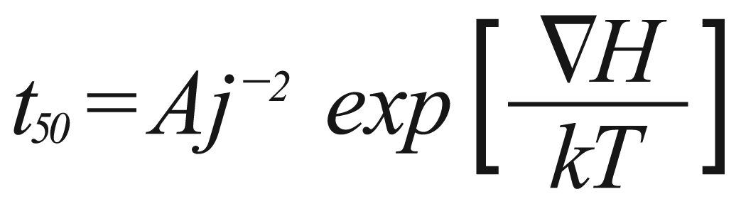
Where t50 is the median time to failure in an ensemble of samples, A is a constant that needs to be empirically determined and DH is the activation energy for failure. The experimental values found for the activation energy suggested grain boundary diffusion as the mass transport mechanism. For nucleation dominated failure, this equation has proven to be adequate even to the present day. Only small corrections, often too small to be detected experimentally have been needed to keep Black’s Law consistent with the latest theoretical developments.
Whether this empirical law holds or not depends entirely on whether the failures are nucleation or growth dominated. This, in turn, depends heavily on the process used to construct the metal lines. If there is no refractory “shunt layer” such as TiN or TiW under the Al line, failure is nucleation dominated and Black's Law holds. If, however, the failures are growth dominated, such as is usually the case for W via failure in narrow lines with shunt layers, Black's Law is not followed and failure times are dependent on 1/j kinetics. Often, as might be expected, the failure process involves both nucleation and growth of damage, and the behavior is more complicated and cannot be described by a simple power law in j.
Wherever growth dominates or is a significant part of the failure time, we assume that 1/j kinetics hold. Most recent experimental data where contacts or vias have been examined in the presence of refractory conductive shunt layers has supported the use of 1/j kinetics, whereas most data on conductor lines attached to bond pads has supported 1/j2 kinetics.