Материал: DS12887
DS12887
RESET is low should exceed 200ms to ensure that the internal timer that controls the DS12887 on power-
up has timed out. When RESET is low and VCC is above 4.25V, the following occurs:
A)Periodic Interrupt Enable (PEI) bit is cleared to 0.
B)Alarm Interrupt Enable (AIE) bit is cleared to 0.
C)Update Ended Interrupt Flag (UF) bit is cleared to 0.
D)Interrupt Request Status Flag (IRQF) bit is cleared to 0.
E)Periodic Interrupt Flag (PF) bit is cleared to 0.
F)The device is not accessible until RESET is returned high.
G)Alarm Interrupt Flag (AF) bit is cleared to 0.
H)H. IRQ pin is in the high impedance state.
I)Square-Wave Output Enable (SQWE ) bit is cleared to 0.
J)Update Ended Interrupt Enable (UIE) is cleared to 0.
In a typical application RESET can be connected to VCC. This connection allows the DS12887 to go in and out of power fail without affecting any of the control registers.
ADDRESS MAP
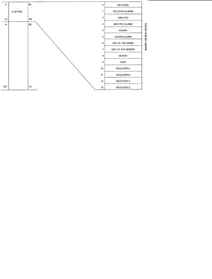
The address map of the DS12887 is shown in Figure 2. The address map consists of 114 bytes of user RAM; 10 bytes of RAM that contain the RTC time, calendar, and alarm data; and 4 bytes that are used for control and status. All 128 bytes can be directly written or read except for the following:
1)Registers C and D are read-only.
2)Bit 7 of Register A is read-only.
3)The high-order bit of the seconds byte is read-only.
The contents of four registers (A, B, C, and D) are described in the Registers section.
Figure 2. ADDRESS MAP
6 of 19

DS12887
TIME, CALENDAR, AND ALARM LOCATIONS
The time and calendar information is obtained by reading the appropriate memory bytes. The time, calendar, and alarm are set or initialized by writing the appropriate RAM bytes. The contents of the 10 time, calendar, and alarm bytes can be either binary or binary coded decimal (BCD) format. Before writing the internal time, calendar, and alarm registers, the SET bit in Register B should be written to a logic 1 to prevent updates from occurring while access is being attempted. In addition to writing the 10 time, calendar, and alarm registers in a selected format (binary or BCD), the data mode bit (DM) of Register B must be set to the appropriate logic level. All 10 time, calendar, and alarm bytes must use the same data mode. The set bit in Register B should be cleared after the data mode bit has been written to allow the RTC to update the time and calendar bytes. Once initialized, the RTC makes all updates in the selected mode. The data mode cannot be changed without reinitializing the 10 data bytes. Table 2 shows the binary and BCD formats of the 10 time, calendar, and alarm locations. The 24–12 bit cannot be changed without reinitializing the hour locations. When the 12-hour format is selected, the high-order bit of the hours byte represents PM when it is a logic 1. The time, calendar, and alarm bytes are always accessible because they are double buffered. The 10 bytes are advanced once per second by 1 second and checked for an alarm condition. If a read of the time and calendar data occurs during an update, a problem exists where seconds, minutes, hours, etc., might not correlate. The probability of reading incorrect time and calendar data is low. Several methods of avoiding any possible incorrect time and calendar reads are covered later in this text.
The three alarm bytes can be used in two ways. First, when the alarm time is written in the appropriate hours, minutes, and seconds alarm locations, the alarm interrupt is initiated at the specified time each day if the alarm enable bit is high. The second use condition is to insert a “don’t care” state in one or more of the three alarm bytes. The “don’t care” code is any hexadecimal value from C0 to FF. The two most significant bits of each byte set the “don’t care” condition when at logic 1. An alarm is generated each hour when the “don’t care” bits are set in the hours byte. Similarly, an alarm is generated every minute with “don’t care” codes in the hours and minute alarm bytes. The “don’t care” codes in all three alarm bytes create an interrupt every second.
Table 2. TIME, CALENDAR, AND ALARM DATA MODES
ADDRESS |
FUNCTION |
DECIMAL |
DATA MODE RANGE |
||
LOCATION |
RANGE |
BINARY |
BCD |
||
|
|||||
0 |
Seconds |
0–59 |
00–3B |
00–59 |
|
1 |
Seconds Alarm |
0–59 |
00–3B |
00–59 |
|
2 |
Minutes |
0–59 |
00–3B |
00–59 |
|
3 |
Minutes Alarm |
0–59 |
00–3B |
00–59 |
|
|
Hours, 12-hour Mode |
1–12 |
01–0C AM, |
01–12AM, |
|
4 |
81–8C PM |
81–92PM |
|||
|
|
||||
|
Hours, 24-hour Mode |
0–23 |
00–17 |
00–23 |
|
|
Hours Alarm, 12-hour |
1–12 |
01–0C AM, |
01–12AM, |
|
5 |
81–8C PM |
81–92PM |
|||
|
|
||||
|
Hours Alarm, 24-hourr |
0–23 |
00–17 |
00–23 |
|
6 |
Day of the Week |
1–7 |
01–07 |
01–07 |
|
Sunday = 1 |
|||||
|
|
|
|
||
7 |
Date of the Month |
1–31 |
01–1F |
01–31 |
|
8 |
Month |
1–12 |
01–0C |
01–12 |
|
9 |
Year |
0–99 |
00–63 |
00–99 |
|
7 of 19

DS12887
NV RAM
The 114 general-purpose NV RAM bytes are not dedicated to any special function within the DS12887. They can be used by the processor program as nonvolatile memory and are fully available during the update cycle.
INTERRUPTS
The RTC plus RAM includes three separate, fully automatic sources of interrupt for a processor. The alarm interrupt can be programmed to occur at rates from once per second to once per day. The periodic interrupt can be selected for rates from 500ms to 122 s. The update-ended interrupt can be used to indicate to the program that an update cycle is complete. Each of these independent interrupt conditions is described in greater detail in other sections of this text.
The processor program can select which interrupts, if any, are going to be used. Three bits in Register B enable the interrupts. Writing a logic 1 to an interrupt-enable bit permits that interrupt to be initiated when the event occurs. A 0 in an interrupt-enable bit prohibits the IRQ pin from being asserted from that interrupt condition. If an interrupt flag is already set when an interrupt is enabled, IRQ is immediately set at an active level, although the interrupt initiating the event may have occurred much earlier. As a result, there are cases where the program should clear such earlier initiated interrupts before first enabling new interrupts.
When an interrupt event occurs, the relating flag bit is set to logic 1 in Register C. These flag bits are set independently of the state of the corresponding enable bit in Register B. The flag bit can be used in a polling mode without enabling the corresponding enable bits. The interrupt flag bit is a status bit that software can interrogate as necessary. When a flag is set, an indication is given to software that an interrupt event has occurred since the flag bit was last read; however, care should be taken when using the flag bits as they are cleared each time Register C is read. Double latching is included with Register C so that set bits remain stable throughout the read cycle. All bits that are set (high) are cleared when read and new interrupts that are pending during the read cycle are held until after the cycle is completed. One, two, or three bits can be set when reading Register C. Each used flag bit should be examined when read to ensure that no interrupts are lost.
The second flag bit usage method is with fully enabled interrupts. When an interrupt flag bit is set and the corresponding interrupt-enable bit is also set, the IRQ pin is asserted low. IRQ is asserted as long as at least one of the three interrupt sources has its flag and enable bits both set. The IRQF bit in Register C is a 1 whenever the IRQ pin is being driven low. Determination that the RTC initiated an interrupt is accomplished by reading Register C. A logic 1 in bit 7 (IRQF bit) indicates that one or more interrupts have been initiated by the DS12887. The act of reading Register C clears all active flag bits and the IRQF bit.
8 of 19

DS12887
OSCILLATOR CONTROL BITS
When the DS12887 is shipped from the factory, the internal oscillator is turned off. This feature prevents the lithium energy cell from being used until it is installed in a system. A pattern of 010 in bits 4 through 6 of Register A turns the oscillator on and enables the countdown chain. A pattern of 11X turns the oscillator on, but holds the countdown chain of the oscillator in reset. All other combinations of bits 4 through 6 keep the oscillator off.
SQUARE-WAVE OUTPUT SELECTION
Thirteen of the 15 divider taps are made available to a 1-of-15 selector, as shown in the block diagram of Figure 1. The first purpose of selecting a divider tap is to generate a square-wave output signal on the SQW pin. The RS0–RS3 bits in Register A establish the square-wave output frequency. These frequencies are listed in Table 1. The SQW frequency selection shares its 1–of–15 selector with the periodic interrupt generator. Once the frequency is selected, the output of the SQW pin can be turned on and off under program control with the square-wave enable bit (SQWE).
PERIODIC INTERRUPT SELECTION
The periodic interrupt causes the IRQ pin to go to an active state from once every 500ms to once every 122 s. This function is separate from the alarm interrupt, which can be output from once per second to once per day. The periodic interrupt rate is selected using the same Register A bits, which select the square-wave frequency (Table 1). Changing the Register A bits affect both the square-wave frequency and the periodic-interrupt output. However, each function has a separate enable bit in Register B. The SQWE bit controls the square-wave output. Similarly, the periodic interrupt is enabled by the PIE bit in Register B. The periodic interrupt can be used with software counters to measure inputs, create output intervals, or await the next needed software function.
UPDATE CYCLE
The DS12887 executes an update cycle once per second regardless of the SET bit in Register B. When the SET bit in Register B is set to 1, the user copy of the double-buffered time, calendar, and alarm bytes is frozen and will not update as the time increments. However, the time countdown chain continues to update the internal copy of the buffer. This feature allows time to maintain accuracy independent of reading or writing the time, calendar, and alarm buffers and also guarantees that time and calendar information is consistent. The update cycle also compares each alarm byte with the corresponding time byte and issues an alarm if a match or if a “don’t care” code is present in all three positions.
There are three methods that can handle access of the RTC that avoid any possibility of accessing inconsistent time and calendar data. The first method uses the update-ended interrupt. If enabled, an interrupt occurs after every update cycle that indicates that over 999ms are available to read valid time and date information. If this interrupt is used, the IRQF bit in Register C should be cleared before leaving the interrupt routine.
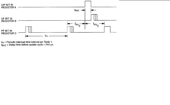
A second method uses the update-in-progress bit (UIP) in Register A to determine if the update cycle is in progress. The UIP bit pulses once per second. After the UIP bit goes high, the update transfer occurs 244 s later. If a low is read on the UIP bit, the user has at least 244 s before the time/calendar data is
9 of 19
DS12887
changed. Therefore, the user should avoid interrupt service routines that would cause the time needed to read valid time/calendar data to exceed 244 s.
The third method uses a periodic interrupt to determine if an update cycle is in progress. The UIP bit in Register A is set high between the setting of the PF bit in Register C (Figure 3). Periodic interrupts that occur at a rate of greater than tBUC allow valid time and date information to be reached at each occurrence of the periodic interrupt. The reads should be complete within one (tPI/2 + tBUC) to ensure that data is not read during the update cycle.
Figure 3. UPDATE-ENDED AND PERIODIC INTERRUPT RELATIONSHIP
10 of 19