Материал: DS12887
DS12887
Real-Time Clock
www.maxim-ic.com
FEATURES
Drop-in replacement for IBM AT computer clock/calendar
Pin-compatible with the MC146818B and DS1287
Totally nonvolatile with over 10 years of operation in the absence of power
Self-contained subsystem includes lithium, quartz, and support circuitry
Counts seconds, minutes, hours, days, day of the week, date, month, and year with leapyear compensation valid up to 2100
Binary or BCD representation of time, calendar, and alarm
12-hour or 24-hour clock with AM and PM in 12-hour mode
Daylight Savings Time option
Selectable between Motorola and Intel bus timing
Multiplex bus for pin efficiency
Interfaced with software as 128 RAM locations
–14 bytes of clock and control registers
–114 bytes of general-purpose RAM
Programmable square-wave output signal
Bus-compatible interrupt signals ( IRQ )
Three interrupts are separately softwaremaskable and testable
–Time-of-day alarm once/second to once/day
–Periodic rates from 122ms to 500ms
–End-of-clock update cycle
Underwriters Laboratory (UL) recognized
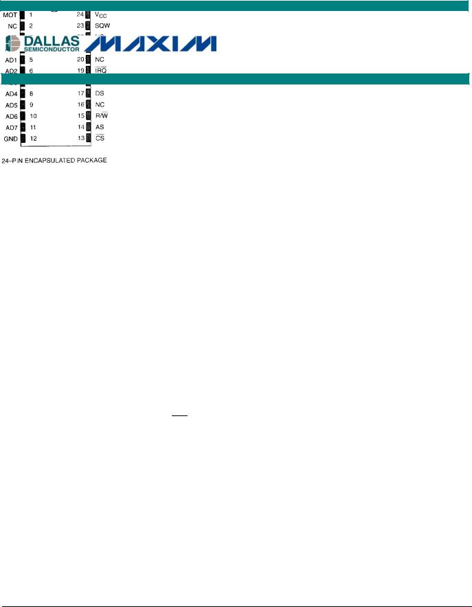
PIN ASSIGNMENT (Top View)
NC
DS12887 24 PDIP Module (700mil)
Package Dimension Information
http://www.maxim-ic.com/TechSupport/DallasPackInfo.htm
PIN DESCRIPTION
AD0–AD7 |
– Multiplexed Address/Data Bus |
||||||
N.C. |
– No Connection |
||||||
MOT |
– Bus Type Selection |
||||||
|
|
|
|
|
|
|
– Chip Select |
|
CS |
||||||
AS |
– Address Strobe |
||||||
R/ |
|
|
|
|
– Read/Write Input |
||
W |
|||||||
DS |
– Data Strobe |
||||||
|
|
|
|
– Reset Input |
|||
|
RESET |
||||||
|
|
|
– Interrupt Request Output |
||||
|
IRQ |
||||||
SQW |
– Square-Wave Output |
||||||
VCC |
– +5V Supply |
||||||
GND |
– Ground |
||||||
ORDERING INFORMATION
PART |
PIN-PACKAGE |
TOP MARK |
TEMP RANGE |
DS12887 |
24 PDIP Module |
DS12887 |
0°C to +70°C |
Note: Some revisions of this device may incorporate deviations from published specifications known as errata. Multiple revisions of any device may be simultaneously available through various sales channels. For information about device errata, click here: http://www.maxim-ic.com/errata.
1 of 19 |
073102 |
DS12887
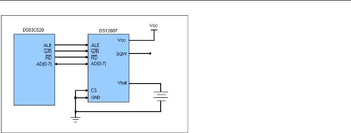
TYPICAL OPERATING CIRCUIT
DESCRIPTION
The DS12887 real-time clock (RTC) plus RAM is designed to be a direct replacement for the DS1287. The DS12887 is identical in form, fit, and function to the DS1287, and has an additional 64 bytes of general-purpose RAM. Access to this additional RAM space is determined by the logic level presented on AD6 during the address portion of an access cycle. A lithium energy source, quartz crystal, and writeprotection circuitry are contained within a 24-pin dual in-line package. As such, the DS12887 is a complete subsystem replacing 16 components in a typical application. The functions include a nonvolatile time-of-day clock, an alarm, a 100-year calendar, programmable interrupt, square-wave generator, and 114 bytes of NV SRAM. The RTC is unique in that time-of-day and memory are maintained even in the absence of power.
OPERATION
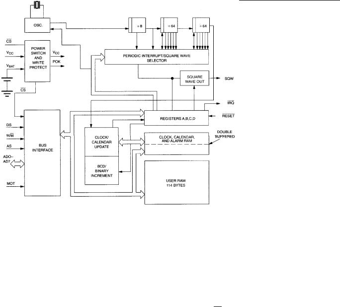
The block diagram in Figure 1 shows the pin connections with the major internal functions of the DS12887. The following paragraphs describe the function of each pin.
2 of 19
DS12887
Figure 1. BLOCK DIAGRAM
POWER-UP/DOWN CONSIDERATIONS
The RTC function continues to operate, and all of the RAM, time, calendar, and alarm memory locations remain nonvolatile regardless of the level of the VCC input. When VCC is applied to the DS12887 and reaches a level of greater than 4.25V, the device becomes accessible after 200ms, provided that the oscillator is running and the oscillator countdown chain is not in reset (Register A). This time period allows the system to stabilize after power is applied. When VCC falls below 4.25V, the chip-select input is
internally forced to an inactive level regardless of the value of CS at the input pin. The DS12887 is, therefore, write-protected. When the DS12887 is in a write-protected state, all inputs are ignored and all outputs are in a high-impedance state. When VCC falls below a level of approximately 3V, the external VCC supply is switched off, and an internal lithium energy source supplies power to the RTC and the RAM memory.
3 of 19

DS12887
SIGNAL DESCRIPTIONS
GND, VCC – DC power is provided to the device on these pins. VCC is the +5V input. When 5V are applied within normal limits, the device is fully accessible and data can be written and read. When VCC is below 4.25V typical, reads and writes are inhibited. However, the timekeeping function continues unaffected by the lower input voltage. As VCC falls below 3V typical, the RAM and timekeeper are switched over to an internal lithium energy source. The timekeeping function maintains an accuracy of 1 minute per month at +25 C, regardless of the voltage input on the VCC pin.
MOT (Mode Select) – The MOT pin offers the flexibility to choose between two bus types. When connected to VCC, Motorola bus timing is selected. When connected to GND or left disconnected, Intel bus timing is selected. The pin has an internal pulldown resistance of approximately 20k .
SQW (Square-Wave Output) – The SQW pin can output a signal from one of 13 taps provided by the 15 internal divider stages of the RTC. The frequency of the SQW pin can be changed by programming Register A, as shown in Table 1. The SQW signal can be turned on and off using the SQWE bit in Register B. The SQW signal is not available when VCC is less than 4.25V, typically.
Table 1. PERIODIC INTERRUPT RATE AND SQUARE-WAVE OUTPUT
FREQUENCY
SELECT BITS REGISTER A |
tPI PERIODIC |
SQW OUTPUT |
|||
RS3 |
RS2 |
RS1 |
RS0 |
INTERRUPT RATE |
FREQUENCY |
0 |
0 |
0 |
0 |
None |
None |
0 |
0 |
0 |
1 |
3.90625ms |
256Hz |
0 |
0 |
1 |
0 |
7.8125ms |
128Hz |
0 |
0 |
1 |
1 |
122.070 s |
8.192kHz |
0 |
1 |
0 |
0 |
244.141 s |
4.096kHz |
0 |
1 |
0 |
1 |
488.281 s |
2.048kHz |
0 |
1 |
1 |
0 |
976.5625 s |
1.024kHz |
0 |
1 |
1 |
1 |
1.953125ms |
512Hz |
1 |
0 |
0 |
0 |
3.90625ms |
256Hz |
1 |
0 |
0 |
1 |
7.8125ms |
128Hz |
1 |
0 |
1 |
0 |
15.625ms |
64Hz |
1 |
0 |
1 |
1 |
31.25ms |
32Hz |
1 |
1 |
0 |
0 |
62.5ms |
16Hz |
1 |
1 |
0 |
1 |
125ms |
8Hz |
1 |
1 |
1 |
0 |
250ms |
4Hz |
1 |
1 |
1 |
1 |
500ms |
2Hz |
AD0–AD7 (Multiplexed Bidirectional Address/Data Bus) – Multiplexed buses save pins because address information and data information time-share the same signal paths. The addresses are present during the first portion of the bus cycle and the same pins and signal paths are used for data in the second portion of the cycle. Address/data multiplexing does not slow the access time of the DS12887 since the bus change from address to data occurs during the internal RAM access time. Addresses must be valid prior to the falling edge of AS/ ALE, at which time the DS12887 latches the address from AD0 to AD6.
Valid write data must be present and held stable during the latter portion of the DS or WR pulses. In a
read cycle the DS12887 outputs 8 bits of data during the latter portion of the DS or RD pulses. The read
4 of 19

DS12887
cycle is terminated and the bus returns to a high-impedance state as DS transitions low in the case of
Motorola timing or as RD transitions high in the case of Intel timing.
AS (Address Strobe Input) – A positive-going address-strobe pulse serves to demultiplex the bus. The falling edge of AS/ALE causes the address to be latched within the DS12887. The next rising edge that
occurs on the AS bus clears the address regardless of whether CS is asserted. Access commands should be sent in pairs.
DS (Data Strobe or Read Input) – The DS/ RD pin has two modes of operation depending on the level of the MOT pin. When the MOT pin is connected to VCC, Motorola bus timing is selected. In this mode, DS is a positive pulse during the latter portion of the bus cycle and is called Data Strobe. During read cycles, DS signifies the time that the DS12887 is to drive the bidirectional bus. In write cycles the trailing edge of DS causes the DS12887 to latch the written data. When the MOT pin is connected to GND, Intel
bus timing is selected. In this mode the DS pin is called Read ( RD ). RD identifies the time period when the DS12887 drives the bus with read data. The RD signal is the same definition as the output-enable (OE ) signal on a typical memory.
R/ W (Read/Write Input) – The R/ W pin also has two modes of operation. When the MOT pin is connected to VCC for Motorola timing, R/ W is at a level that indicates whether the current cycle is a read or write. A read cycle is indicated with a high level on R/ W while DS is high. A write cycle is indicated when R/ W is low during DS.
When the MOT pin is connected to GND for Intel timing, the R/ W signal is an active-low signal called
WR. In this mode, the R/ W pin has the same meaning as the write-enable signal ( WE ) on generic RAMs.
CS (Chip-Select Input) – The chip select signal must be asserted low for a bus cycle in the DS12887 to
be accessed. CS must be kept in the active state during DS and AS for Motorola timing and during RD
and WR for Intel timing. Bus cycles that take place without asserting CS latch addresses but no access occur. When VCC is below 4.25V, the DS12887 internally inhibits access cycles by internally disabling
the CS input. This action protects both the RTC data and RAM data during power outages.
IRQ (Interrupt Request Output) – The IRQ pin is an active-low output of the DS12887 that can be
used as an interrupt input to a processor. The IRQ output remains low as long as the status bit causing the
interrupt is present and the corresponding interrupt-enable bit is set. To clear the IRQ pin, the processor
program normally reads the C register. The RESET pin also clears pending interrupts.
When no interrupt conditions are present, the IRQ level is in the high-impedance state. Multiple
interrupting devices can be connected to an IRQ bus. The IRQ bus is an open drain output and requires an external pullup resistor.
RESET (Reset Input) – The RESET pin has no affect on the clock, calendar, or RAM. On power-up, the RESET pin can be held low for a time to allow the power supply to stabilize. The amount of time that RESET is held low is dependent on the application. However, if RESET is used on power-up, the time
5 of 19