Материал: 8951l
Features
• Compatible with MCS-51™ Products
•4K Bytes of Reprogrammable Flash Memory
-Endurance: 1,000 Write/Erase Cycles
•2.7V to 6V Operating Range
•Fully Static Operation: 0 Hz to 12 MHz
•Three-Level Program Memory Lock
•128 x 8-Bit Internal RAM
•32 Programmable I/O Lines
•Two 16-Bit Timer/Counters
•Six Interrupt Sources
•Programmable Serial Channel
•Low Power Idle and Power Down Modes
Description
The AT89LV51 is a low-voltage, high-performance CMOS 8-bit microcomputer with 4K bytes of Flash Programmable and Erasable Read Only Memory. The device is manufactured using Atmel's high density nonvolatile memory technology and is compatible with the industry standard MCS-51™ instruction set and pinout. The on-chip Flash allows the program memory to be reprogrammed in-system or by a conventional nonvolatile memory programmer. By combining a versatile 8-bit CPU with Flash on a monolithic chip, the Atmel AT89LV51 is a powerful microcomputer which provides a highly flexible and cost effective solution to many embedded control applica-
tions. |
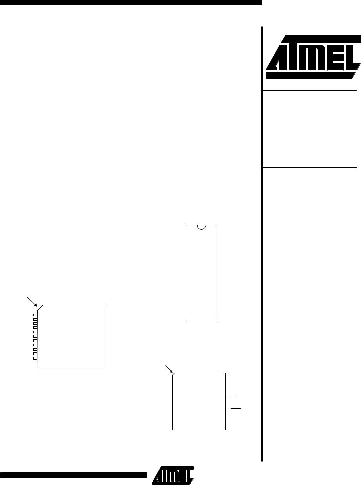
PDIP |
|
Pin Configurations
I N D E X
C O R N E R
|
|
|
|
|
P 1 . 5 |
|
|
|
|
|
P 1 . 6 |
|
|
|
|
|
P 1 . 7 |
|
|
|
|
|
R S T |
( R X D ) |
P 3 . 0 |
||||
|
|
|
|
|
N C |
|
|
( T X D ) |
P 3 . 1 |
||
( |
|
|
|
) |
P 3 . 2 |
I N T 0 |
|||||
( |
I N T 1 |
) |
P 3 . 3 |
||
|
|
( T 0 ) |
P 3 . 4 |
||
|
|
( T 1 ) |
P 3 . 5 |
||
TQFP
|
|
|
|
|
|
|
|
|
|
|
|
|
|
(AD0) (AD1) (AD2) (AD3) |
|
|
|
|
|
|
|
|
|
||||||||
|
1.4 1.3 1.2 1.1 1.0 C |
CC |
0.0 0.1 0.2 0.3 |
|
|
|
|
|
|
|
|
|
|
||||||||||||||||||
|
P P P P P N |
V |
P P P P |
|
|
|
|
|
|
|
|
|
|||||||||||||||||||
|
|
|
|
|
|
|
|
|
|
|
|
|
|
|
|
|
|
|
|
|
|
|
|
|
|
|
|
|
|
|
|
4 4 |
|
|
4 2 |
4 0 |
|
|
3 8 |
3 6 |
3 4 |
|
|
|
|
|
|
|
|
|
|||||||||||||
4 3 |
|
|
4 1 |
|
3 9 |
|
3 7 |
|
3 5 |
|
|
|
|
|
|
|
|
|
|
|
|||||||||||
1 |
|
|
|
|
|
|
|
|
|
|
|
|
|
|
|
|
|
3 3 |
|
|
P 0 . 4 ( A D 4 ) |
||||||||||
2 |
|
|
|
|
|
|
|
|
|
|
|
|
|
|
|
|
|
3 2 |
|
|
P 0 . 5 ( A D 5 ) |
||||||||||
3 |
|
|
|
|
|
|
|
|
|
|
|
|
|
|
|
|
|
3 1 |
|
|
P 0 . 6 ( A D 6 ) |
||||||||||
4 |
|
|
|
|
|
|
|
|
|
|
|
|
|
|
|
|
|
3 0 |
|
|
P 0 . 7 ( A D 7 ) |
||||||||||
5 |
|
|
|
|
|
|
|
|
|
|
|
|
|
|
|
|
|
2 9 |
|
|
|
|
|
|
|
|
|
||||
|
|
|
|
|
|
|
|
|
|
|
|
|
|
|
|
|
|
|
E A / V P P |
||||||||||||
|
|
|
|
|
|
|
|
|
|
|
|
|
|
|
|
|
|
|
|||||||||||||
6 |
|
|
|
|
|
|
|
|
|
|
|
|
|
|
|
|
|
2 8 |
|
|
N C |
||||||||||
7 |
|
|
|
|
|
|
|
|
|
|
|
|
|
|
|
|
|
2 7 |
|
|
|
|
G |
||||||||
|
|
|
|
|
|
|
|
|
|
|
|
|
|
|
|
|
|
|
A L E / P R O |
||||||||||||
|
|
|
|
|
|
|
|
|
|
|
|
|
|
|
|
|
|
|
|
|
|
|
|
|
|
|
|
||||
8 |
|
|
|
|
|
|
|
|
|
|
|
|
|
|
|
|
|
2 6 |
|
|
P S E N |
||||||||||
9 |
|
|
|
|
|
|
|
|
|
|
|
|
|
|
|
|
|
2 5 |
|
|
P 2 . 7 ( A 1 5 ) |
||||||||||
1 0 |
|
|
|
|
|
|
|
|
|
|
|
|
|
|
|
|
|
2 4 |
|
|
P 2 . 6 ( A 1 4 ) |
||||||||||
1 1 |
|
|
|
|
|
|
|
|
|
|
|
|
|
|
|
|
|
2 3 |
|
|
P 2 . 5 ( A 1 3 ) |
||||||||||
1 21 31 41 51 61 71 81 92 02 12 2 |
|
|
|
|
|
|
|
|
|
||||||||||||||||||||||
|
|
|
|
|
|
|
|
|
|
|
|
|
|
|
|
|
|
|
|
|
|
|
|
|
|
|
|
|
|
|
|
|
P3.6 P3.7 TAL2 TAL1 GND GND P2.0 P2.1 P2.2 P2.3 P2.4 |
|
|
|
|
|
|
|
|
|
|||||||||||||||||||||
|
) |
|
) X X |
|
|
) ) ) ) ) |
|
|
|
|
|
|
|
|
|
|
|||||||||||||||
|
(WR |
|
(RD |
|
|
|
|
|
|
|
|
(A8 (A9 (A10 (A11 (A12 |
|
|
|
|
|
|
|
|
|
||||||||||
|
|
|
|
|
|
|
|
|
|
|
|
|
|
|
|
|
|
|
|||||||||||||
|
|
|
|
|
P 1 . 0 |
|
1 |
4 0 |
|
|
V C C |
||||
|
|
||||||||||||||
|
|
|
|
|
P 1 . 1 |
|
2 |
3 9 |
|
|
P 0 . 0 ( A D 0 ) |
||||
|
|
||||||||||||||
|
|
|
|
|
P 1 . 2 |
|
3 |
3 8 |
|
|
P 0 . 1 ( A D 1 ) |
||||
|
|
||||||||||||||
|
|
|
|
|
P 1 . 3 |
|
4 |
3 7 |
|
|
P 0 . 2 ( A D 2 ) |
||||
|
|
||||||||||||||
|
|
|
|
|
P 1 . 4 |
|
5 |
3 6 |
|
|
P 0 . 3 ( A D 3 ) |
||||
|
|
||||||||||||||
|
|
|
|
|
P 1 . 5 |
|
6 |
3 5 |
|
|
P 0 . 4 ( A D 4 ) |
||||
|
|
||||||||||||||
|
|
|
|
|
P 1 . 6 |
|
7 |
3 4 |
|
|
P 0 . 5 ( A D 5 ) |
||||
|
|
|
|
|
P 1 . 7 |
|
8 |
3 3 |
|
|
P 0 . 6 ( A D 6 ) |
||||
|
|
||||||||||||||
|
|
|
|
|
R S T |
|
9 |
3 2 |
|
|
P 0 . 7 ( A D 7 ) |
||||
|
|
||||||||||||||
( R X D ) P 3 . 0 |
|
1 0 |
3 1 |
|
|
E A |
/ V P P |
||||||||
|
|
||||||||||||||
( T X D ) P 3 . 1 |
|
1 1 |
3 0 |
|
|
A L E / |
P R O G |
|
|||||||
|
|
||||||||||||||
( |
I N T 0 |
) P 3 . 2 |
|
1 2 |
2 9 |
|
|
P S E N |
|
||||||
|
|
||||||||||||||
( |
I N T 1 |
) P 3 . 3 |
|
1 3 |
2 8 |
|
|
P 2 . 7 ( A 1 5 ) |
|||||||
|
|
||||||||||||||
|
( T 0 ) P 3 . 4 |
|
1 4 |
2 7 |
|
|
P 2 . 6 ( A 1 4 ) |
||||||||
|
|
||||||||||||||
|
( T 1 ) P 3 . 5 |
|
1 5 |
2 6 |
|
|
P 2 . 5 ( A 1 3 ) |
||||||||
|
|
||||||||||||||
|
( |
W R |
) P 3 . 6 |
|
1 6 |
2 5 |
|
|
P 2 . 4 ( A 1 2 ) |
||||||
|
|
||||||||||||||
|
( |
R D |
) P 3 . 7 |
|
1 7 |
2 4 |
|
|
P 2 . 3 ( A 1 1 ) |
||||||
|
|
||||||||||||||
|
|
|
|
|
X TA L 2 |
|
1 8 |
2 3 |
|
|
P 2 . 2 ( A 1 0 ) |
||||
|
|
||||||||||||||
|
|
|
|
|
X TA L 1 |
|
1 9 |
2 2 |
|
|
P 2 . 1 ( A 9 ) |
||||
|
|
||||||||||||||
|
|
|
|
|
G N D |
|
2 0 |
2 1 |
|
|
P 2 . 0 ( A 8 ) |
||||
PLCC
|
|
|
|
|
|
|
|
|
|
|
|
|
|
|
|
|
|
|
|
|
|
|
|
|
(AD0) (AD1) (AD2) (AD3) |
|
|
|
|
|
||||||||
|
|
I N D E X |
|
|
.1P4 .1P3 .1P2 .1P1 |
.1P0 CN |
CVC |
0P.0 0P.1 0P.2 0P.3 |
|
|
|
|
|
|||||||||||||||||||||||||
|
|
C O R N E R |
|
|
|
|
|
|
|
|||||||||||||||||||||||||||||
|
|
|
|
|
|
|
|
|
|
|
|
|
|
|
|
|
|
|
|
|
|
|
|
|
|
|
|
|
|
|
|
|
|
|
|
|
||
|
|
|
|
|
|
|
|
|
|
|
|
|
|
|
|
|
|
|
|
|
|
|
|
|
|
|
|
|
|
|
|
|
|
|
|
|
||
|
|
|
|
|
|
|
|
|
|
|
|
|
|
|
|
|
|
|
|
|
|
|
|
|
|
|
|
|
|
|
|
|
|
|
|
|
||
|
|
|
|
6 |
|
|
4 |
|
|
2 |
|
4 4 |
4 2 |
|
4 0 |
|
|
|
|
|
||||||||||||||||||
|
|
|
P 1 . 5 |
|
|
7 |
|
5 3 |
|
1 4 3 4 1 3 9 |
|
|
P 0 . 4 ( A D 4 ) |
|||||||||||||||||||||||||
|
|
|
P 1 . 6 |
|
|
8 |
|
|
|
|
|
|
|
|
|
|
|
|
|
|
|
|
|
|
|
|
|
|
|
|
3 8 |
|
|
P 0 . 5 ( A D 5 ) |
||||
|
|
|
|
|
|
|
|
|
|
|
|
|
|
|
|
|
|
|
|
|
|
|
|
|
|
|
|
|
|
|
|
|
|
|||||
|
|
|
P 1 . 7 |
|
9 |
|
|
|
|
|
|
|
|
|
|
|
|
|
|
|
|
|
|
|
|
|
|
|
|
3 7 |
|
|
P 0 . 6 ( A D 6 ) |
|||||
|
|
|
|
|
|
|
|
|
|
|
|
|
|
|
|
|
|
|
|
|
|
|
|
|
|
|
|
|
|
|
|
|
|
|||||
|
|
|
R S T |
|
1 0 |
|
|
|
|
|
|
|
|
|
|
|
|
|
|
|
|
|
|
|
|
|
|
|
3 6 |
|
|
P 0 . 7 ( A D 7 ) |
||||||
|
|
|
|
|
|
|
|
|
|
|
|
|
|
|
|
|
|
|
|
|
|
|
|
|
|
|
|
|
|
|||||||||
( R X D ) P 3 . 0 |
|
1 1 |
|
|
|
|
|
|
|
|
|
|
|
|
|
|
|
|
|
|
|
|
|
|
|
3 5 |
|
|
E A / V P P |
|||||||||
|
|
|
N C |
|
1 2 |
|
|
|
|
|
|
|
|
|
|
|
|
|
|
|
|
|
|
|
|
|
|
|
3 4 |
|
|
N C |
||||||
( T X D ) P 3 . 1 |
|
1 3 |
|
|
|
|
|
|
|
|
|
|
|
|
|
|
|
|
|
|
|
|
|
|
|
3 3 |
|
|
A L E / |
|
|
|||||||
|
|
|
|
|
|
|
|
|
|
|
|
|
|
|
|
|
|
|
|
|
|
|
P R O G |
|||||||||||||||
( |
|
|
) P 3 . 2 |
|
|
1 4 |
|
|
|
|
|
|
|
|
|
|
|
|
|
|
|
|
|
|
|
|
|
|
|
3 2 |
|
|
P S E N |
|||||
I N T 0 |
|
|
|
|
|
|
|
|
|
|
|
|
|
|
|
|
|
|
|
|
|
|
|
|||||||||||||||
( |
|
|
) P 3 . 3 |
|
|
1 5 |
|
|
|
|
|
|
|
|
|
|
|
|
|
|
|
|
|
|
|
|
|
|
|
3 1 |
|
|
P 2 . 7 ( A 1 5 ) |
|||||
I N T 1 |
|
|
|
|
|
|
|
|
|
|
|
|
|
|
|
|
|
|
|
|
|
|
|
|||||||||||||||
|
|
|
|
|
|
|
|
|
|
|
|
|
|
|
|
|
|
|
|
|
|
|
|
|
|
|
||||||||||||
|
|
( T 0 ) P 3 . 4 |
|
1 6 |
|
|
|
|
|
|
|
|
|
|
|
|
|
|
|
|
|
|
|
|
|
|
|
3 0 |
|
|
P 2 . 6 ( A 1 4 ) |
|||||||
|
|
|
|
|
|
|
|
|
|
|
|
|
|
|
|
|
|
|
|
|
|
|
|
|
|
|
|
|||||||||||
|
|
( T 1 ) P 3 . 5 |
|
1 7 |
1 9 2 1 |
2 3 |
|
2 5 2 7 2 9 |
|
|
P 2 . 5 ( A 1 3 ) |
|||||||||||||||||||||||||||
|
|
|
|
1 8 |
2 0 |
|
|
|
2 2 |
|
|
2 4 |
2 6 |
|
2 8 |
|
|
|
|
|
||||||||||||||||||
|
|
|
|
|
|
|
|
|
|
|
|
|
|
|
|
|
|
|
|
|
|
|
|
P3.6 P3.7 TAL2 TAL1 GND NC P2.0 P2.1 P2.2 P2.3 P2.4 |
|||||||||||||||||||||
|
(WR) (RD) |
|
X X |
(A8) (A9) (A10) (A11) (A12) |
||||||||||||||||||
|
|
|||||||||||||||||||||
|
||||||||||||||||||||||
|
|
|
|
|
|
|
|
|
|
|||||||||||||
AT89LV51
8-Bit Microcontroller with 4K Bytes Flash
AT89LV51
1
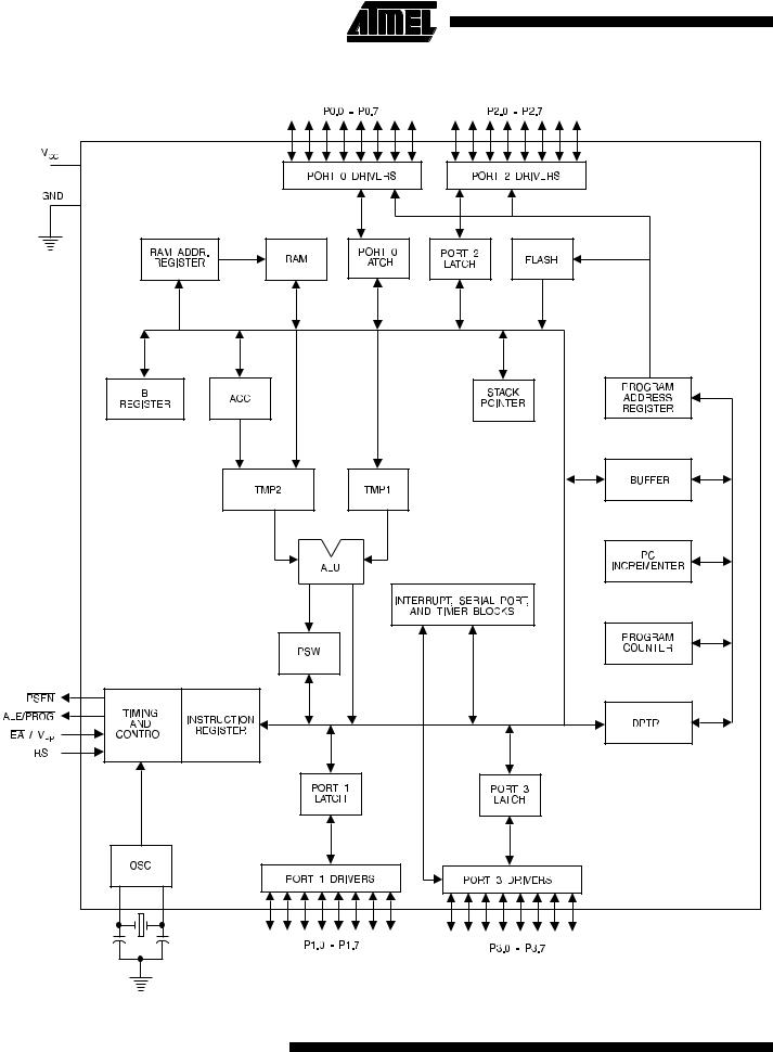
Block Diagram |
|
2 |
AT89LV51 |

The AT89LV51 provides the following standard features: 4K bytes of Flash, 128 bytes of RAM, 32 I/O lines, two 16 bit timer/counters, a five vector two-level interrupt architecture, a full duplex serial port, on-chip oscillator and clock circuitry. In addition, the AT89LV51 is designed with static logic for operation down to zero frequency and supports two software selectable power saving modes. The Idle Mode stops the CPU while allowing the RAM, timer/ counters, serial port and interrupt system to continue functioning. The Power Down Mode saves the RAM contents but freezes the oscillator disabling all other chip functions until the next hardware reset.
Pin Description
VCC
Supply voltage.
GND
Ground.
Port 0
Port 0 is an 8-bit open drain bidirectional I/O port. As an output port each pin can sink eight TTL inputs. When 1s are written to port 0 pins, the pins can be used as highimpedance inputs.
Port 0 may also be configured to be the multiplexed loworder address/data bus during accesses to external program and data memory. In this mode P0 has internal pullups.
Port 0 also receives the code bytes during Flash programming, and outputs the code bytes during program verification. External pullups are required during program verification.
Port 1
Port 1 is an 8 bit bidirectional I/O port with internal pullups. The Port 1 output buffers can sink/source four TTL inputs. When 1s are written to Port 1 pins they are pulled high by the internal pullups and can be used as inputs. As inputs, Port 1 pins that are externally being pulled low will source current (IIL) because of the internal pullups.
Port 1 also receives the low-order address bytes during Flash programming and verification.
Port 2
Port 2 is an 8-bit bidirectional I/O port with internal pullups. The Port 2 output buffers can sink/source four TTL inputs. When 1s are written to Port 2 pins they are pulled high by the internal pullups and can be used as inputs. As inputs, Port 2 pins that are externally being pulled low will source current (IIL) because of the internal pullups.
Port 2 emits the high-order address byte during fetches from external program memory and during accesses to external data memory that use 16 bit addresses (MOVX @ DPTR). In this application it uses strong internal pullups
AT89LV51
when emitting 1s. During accesses to external data memory that use 8-bit addresses (MOVX @ RI), Port 2 emits the contents of the P2 Special Function Register.
Port 2 also receives the high-order address bits and some control signals during Flash programming and verification.
Port 3
Port 3 is an 8-bit bidirectional I/O port with internal pullups. The Port 3 output buffers can sink/source four TTL inputs. When 1s are written to Port 3 pins they are pulled high by the internal pullups and can be used as inputs. As inputs, Port 3 pins that are externally being pulled low will source current (IIL) because of the pullups.
Port 3 also serves the functions of various special features of the AT89LV51 as listed below:
Port Pin |
|
|
Alternate Functions |
|||
|
|
|
|
|||
P3.0 |
|
|
RXD (serial input port) |
|||
P3.1 |
|
|
TXD (serial output port) |
|||
P3.2 |
|
|
|
|
|
(external interrupt 0) |
|
|
INT0 |
||||
P3.3 |
|
|
|
|
|
(external interrupt 1) |
INT1 |
||||||
P3.4 |
T0 (timer 0 external input) |
|||||
P3.5 |
T1 (timer 1 external input) |
|||||
P3.6 |
|
|
|
(external data memory write strobe) |
||
|
WR |
|||||
P3.7 |
|
|
(external data memory read strobe) |
|||
RD |
||||||
|
|
|
|
|
|
|
Port 3 also receives some control signals for Flash programming and verification.
RST
Reset input. A high on this pin for two machine cycles while the oscillator is running resets the device.
ALE/PROG
Address Latch Enable output pulse for latching the low byte of the address during accesses to external memory. This pin is also the program pulse input (PROG) during Flash programming.
In normal operation ALE is emitted at a constant rate of 1/ 6 the oscillator frequency, and may be used for external timing or clocking purposes. Note, however, that one ALE pulse is skipped during each access to external Data Memory.
PSEN
Program Store Enable is the read strobe to external program memory.
When the AT89LV51 is executing code from external program memory, PSEN is activated twice each machine cycle, except that two PSEN activations are skipped during each access to external data memory.
3
EA/VPP
External Access Enable. EA must be strapped to GND in order to enable the device to fetch code from external program memory locations starting at 0000H up to FFFFH. Note, however, that if lock bit 1 is programmed, EA will be internally latched on reset.
EA should be strapped to VCC for internal program executions.
This pin also receives the 12-volt programming enable voltage (VPP) during Flash programming, when 12-volt programming is selected.
XTAL1
Input to the inverting oscillator amplifier and input to the internal clock operating circuit.
XTAL2
Output from the inverting oscillator amplifier.
Table 1. AT89LV51 SFR Map and Reset Values
Special Function Registers
A map of the on-chip memory area called the Special Function Register (SFR) space is shown in Table 1.
Note that not all of the addresses are occupied, and unoccupied addresses may not be implemented on the chip. Read accesses to these addresses will in general return random data, and write accesses will have an indeterminate effect.
User software should not write 1s to these unlisted locations, since they may be used in future products to invoke new features. In that case, the reset or inactive values of the new bits will always be 0.
Timer 0 and 1
Timer 0 and Timer 1 in the AT89LV51 operate the same way as Timer 0 and Timer 1 in the AT89C51.
0F8H
0F0H
0E8H
0E0H
0D8H
0D0H
0C8H
0C0H
0B8H
0B0H
0A8H
0A0H
98H
90H
88H
80H
|
|
|
|
|
|
|
|
0FFH |
|
|
|
|
|
|
|
|
|
B |
|
|
|
|
|
|
|
0F7H |
00000000 |
|
|
|
|
|
|
|
|
|
|
|
|
|
|
|
|
|
|
|
|
|
|
|
|
|
0EFH |
|
|
|
|
|
|
|
|
|
ACC |
|
|
|
|
|
|
|
0E7H |
00000000 |
|
|
|
|
|
|
|
|
|
|
|
|
|
|
|
|
|
|
|
|
|
|
|
|
|
0DFH |
|
|
|
|
|
|
|
|
|
PSW |
|
|
|
|
|
|
|
0D7H |
00000000 |
|
|
|
|
|
|
|
|
|
|
|
|
|
|
|
|
|
T2CON |
T2MOD |
RCAP2L |
RCAP2H |
TL2 |
TH2 |
|
|
0CFH |
00000000 |
XXXXXX00 |
00000000 |
00000000 |
00000000 |
00000000 |
|
|
|
|
|
|
||||||
|
|
|
|
|
|
|
|
0C7H |
|
|
|
|
|
|
|
|
|
IP |
|
|
|
|
|
|
|
0BFH |
XX000000 |
|
|
|
|
|
|
|
|
|
|
|
|
|
|
|
|
|
P3 |
|
|
|
|
|
|
|
0B7H |
11111111 |
|
|
|
|
|
|
|
|
|
|
|
|
|
|
|
|
|
IE |
|
|
|
|
|
|
|
0AFH |
0X000000 |
|
|
|
|
|
|
|
|
|
|
|
|
|
|
|
|
|
P2 |
|
|
|
|
|
|
|
0A7H |
11111111 |
|
|
|
|
|
|
|
|
|
|
|
|
|
|
|
|
|
SCON |
SBUF |
|
|
|
|
|
|
9FH |
00000000 |
XXXXXXXX |
|
|
|
|
|
|
|
|
|
|
|
|
|
|
||
P1 |
|
|
|
|
|
|
|
97H |
11111111 |
|
|
|
|
|
|
|
|
|
|
|
|
|
|
|
|
|
TCON |
TMOD |
TL0 |
TL1 |
TH0 |
TH1 |
|
|
8FH |
00000000 |
00000000 |
00000000 |
00000000 |
00000000 |
00000000 |
|
|
|
|
|
|
||||||
P0 |
SP |
DPL |
DPH |
|
|
|
PCON |
87H |
11111111 |
00000111 |
00000000 |
00000000 |
|
|
|
0XXX0000 |
|
|
|
|
|
4 |
AT89LV51 |
|
|
||
|
Oscillator Characteristics
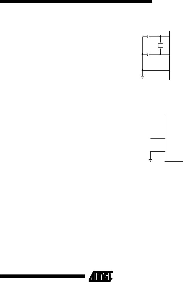
XTAL1 and XTAL2 are the input and output, respectively, of an inverting amplifier which can be configured for use as an on-chip oscillator, as shown in Figure 1. Either a quartz crystal or ceramic resonator may be used. To drive the device from an external clock source, XTAL2 should be left unconnected while XTAL1 is driven as shown in Figure 2. There are no requirements on the duty cycle of the external clock signal, since the input to the internal clocking circuitry is through a divide-by-two flip-flop, but minimum and maximum voltage high and low time specifications must be observed
Idle Mode
In idle mode, the CPU puts itself to sleep while all the onchip peripherals remain active. The mode is invoked by software. The content of the on-chip RAM and all the special functions registers remain unchanged during this mode. The idle mode can be terminated by any enabled interrupt or by a hardware reset.
It should be noted that when idle is terminated by a hardware reset, the device normally resumes program execution, from where it left off, up to two machine cycles before the internal reset algorithm takes control. On-chip hardware inhibits access to internal RAM in this event, but access to the port pins is not inhibited. To eliminate the possibility of an unexpected write to a port pin when Idle is terminated by reset, the instruction following the one that invokes Idle should not be one that writes to a port pin or to external memory.
AT89LV51
Figure 1. Oscillator Connections
C2
XTAL2
C1
XTAL1
GND
Notes: C1, C2 = 30 pF ± 10 pF for Crystals
= 40 pF ± 10 pF for Ceramic Resonators
Figure 2. External Clock Drive Configuration
NC |
|
XTAL2 |
|
EXTERNAL
OSCILLATOR XTAL1
SIGNAL
GND
5