Материал: MJE18204
MJE18204 MJF18204
TYPICAL STATIC CHARACTERISTICS
|
1100 |
IBoff = IB2 |
TJ = 125°C |
|
|
|
1000 |
|
|
||
|
VCC = 15 V |
TJ = 25°C |
|
|
|
|
900 |
|
|
||
|
VZ = 300 V |
|
|
|
|
|
800 |
LC = 200 μH |
|
|
tc |
(ns) |
700 |
|
|
|
|
|
|
|
|
||
|
|
|
|
|
|
t, TIME |
600 |
|
|
|
|
500 |
|
|
|
|
|
|
400 |
|
|
|
|
|
300 |
|
|
|
tfi |
|
200 |
|
|
|
|
|
|
|
|
|
|
|
100 |
1 |
|
|
|
|
0 |
2 |
3 |
4 |
IC, COLLECTOR CURRENT (AMPS)
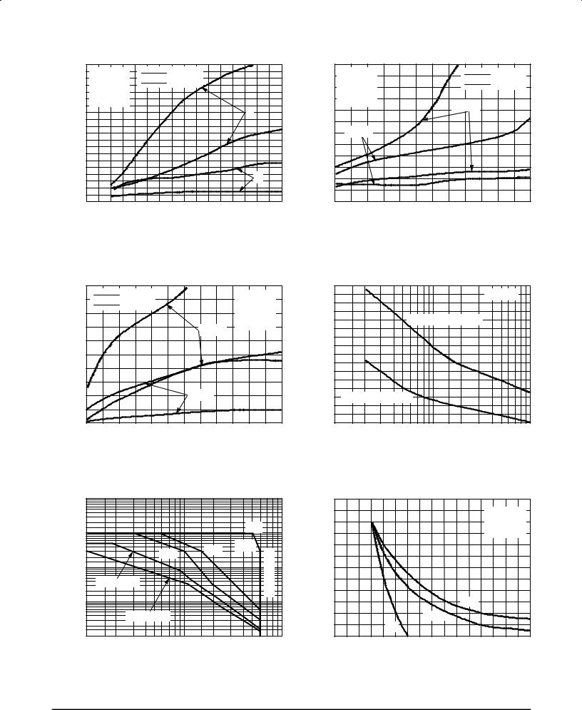
Figure 13. Inductive Switching,
|
|
|
|
|
tc & tfi @ IC/IB = 10 |
|
|
|
|
|
|
||||
|
1200 |
|
|
TJ = 125°C |
|
|
|
|
|
|
|
|
|
|
|
|
|
|
|
|
|
|
|
|
I |
= I |
B2 |
|
|||
|
|
|
|
TJ = 25°C |
|
|
|
|
|
B1 |
|
|
|
||
|
|
|
|
|
|
|
|
|
V |
|
= 15 V |
|
|||
|
1000 |
|
|
|
|
|
|
|
|
|
CC |
|
|
|
|
(ns) |
|
|
|
|
|
|
|
|
|
VZ |
= 300 V |
|
|||
|
|
|
|
|
|
|
|
|
|
|
|||||
|
|
|
|
|
|
|
|
|
|
LC |
= 200 μH |
|
|||
TIME |
|
|
|
|
|
|
|
IC = 2 A |
|
|
|||||
800 |
|
|
|
|
|
|
|
|
|
|
|
|
|||
, CROSSOVER |
|
|
|
|
|
|
|
|
|
|
|
|
|
|
|
600 |
|
|
|
|
|
|
|
|
|
|
|
|
|
|
|
|
|
|
|
|
|
|
|
|
|
|
|
|
|
|
|
c |
|
|
|
|
|
|
|
|
|
|
|
|
|
|
|
t |
400 |
|
|
|
|
|
|
IC = 1 A |
|
|
|
|
|
|
|
|
|
|
|
|
|
|
|
|
|
|
|
|
|
||
|
200 |
|
|
|
|
|
|
|
|
|
|
|
|
|
|
|
3 |
4 |
5 |
6 |
7 |
8 |
9 |
10 |
11 |
12 |
13 |
14 |
15 |
||
hFE, FORCED GAIN
Figure 15. Inductive Crossover Time
|
100 |
|
|
|
(AMPS) |
10 |
|
1 μs |
|
COLLECTOR CURRENT |
|
|
10 μs |
EXTENDED SOA |
|
5 ms |
1 ms |
||
|
|
|||
1 |
|
|
||
|
MJE18204±DC |
|
||
0.1 |
|
|
||
|
|
|
||
, |
|
|
|
|
C |
|
MJF18204±DC |
|
|
I |
|
|
|
|
|
|
|
|
|
|
0.01 |
|
100 |
|
|
10 |
|
1000 |
|
|
|
VCE, COLLECTOR±EMITTER VOLTAGE (VOLTS) |
|
|
Figure 17. Forward Bias Safe Operating Area
|
680 |
|
|
|
|
|
|
|
|
IBoff = IB2 |
|
|
|
TJ = 125°C |
|||
|
V |
CC |
= 15 V |
|
|
|
TJ = 25 |
° |
|
|
|
|
|
|
C |
||
|
VZ = 300 V |
|
|
|
|
|
||
TIME (ns) |
LC = 200 μH |
|
|
IC = 2 A |
|
|
||
480 |
|
|
|
|
|
|
|
|
|
IC = 1 A |
|
|
|
|
|
||
, FALL |
|
|
|
|
|
|
||
280 |
|
|
|
|
|
|
|
|
fi |
|
|
|
|
|
|
|
|
t |
|
|
|
|
|
|
|
|
|
80 |
|
5 |
|
|
11 |
13 |
|
|
3 |
|
7 |
9 |
15 |
|||
hFE, FORCED GAIN
Figure 14. Inductive Fall Time
|
1400 |
|
TJ = 25°C |
|
1300 |
|
|
|
|
|
|
|
1200 |
BVCER (VOLTS) @ 10 mA |
|
(VOLTS) |
1100 |
|
|
1000 |
|
|
|
BVCER |
|
|
|
900 |
|
|
|
|
|
|
|
|
800 |
|
|
|
700 |
BVCER(sus) @ 200 mA |
|
|
|
|
|
|
600 |
|
|
|
10 |
100 |
1000 |
|
|
RBE (Ω) |
|
Figure 16. BVCER = f (RBE)
|
6 |
|
|
|
|
|
|
|
|
(AMPS) |
5 |
|
|
|
|
|
TC ≤ 125°C |
|
|
|
|
|
|
|
GAIN ≥ 5 |
|
|||
|
|
|
|
|
|
LC = 4 mH |
|
||
CURRENT |
4 |
|
|
|
|
|
|
|
|
3 |
|
|
|
|
|
|
|
|
|
, COLLECTOR |
|
|
|
|
|
|
|
|
|
2 |
|
|
|
|
|
|
|
|
|
|
|
|
|
|
|
± 5 V |
|
|
|
1 |
|
|
|
|
|
|
|
|
|
C |
|
|
|
±1.5 V |
|
|
|
|
|
I |
|
|
|
|
|
|
|
||
|
|
|
|
|
|
|
|
|
|
|
0 |
|
0 V |
|
|
|
|
|
|
|
|
600 |
|
|
|
|
|
|
|
|
400 |
500 |
700 |
800 |
900 |
1000 |
1100 |
1200 |
|
|
|
VCE, COLLECTOR±EMITTER VOLTAGE (VOLTS) |
|
||||||
Figure 18. Reverse Bias Switching Safe
Operating Area
6 |
Motorola Bipolar Power Transistor Device Data |
MJE18204 MJF18204
TYPICAL STATIC CHARACTERISTICS
|
1.0 |
|
|
|
|
|
|
|
|
|
|
|
|
|
|
SECOND |
|
FACTOR |
0.8 |
|
|
|
|
|
BREAKDOWN |
|
|
|
|
|
|
|
DERATING |
|
|
0.6 |
|
|
|
|
|
|
|
|
DERATING |
|
|
|
|
|
|
|
|
0.4 |
|
|
|
|
|
|
|
|
POWER |
0.2 |
|
|
|
THERMAL |
|
|
|
|
|
|
|
DERATING |
|
|
|
|
|
|
|
|
|
|
|
|
|
|
0 |
|
|
|
|
|
|
|
|
20 |
40 |
60 |
80 |
100 |
120 |
140 |
160 |
|
|
|
TC, CASE TEMPERATURE (°C) |
|
|
|||
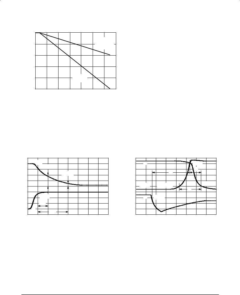
Figure 19. Forward Bias Power Derating
There are two limitations on the power handling ability of a transistor: average junction temperature and second breakdown. Safe operating area curves indicate IC±VCE limits of the transistor that must be observed for reliable operation; i.e., the transistor must not be subjected to greater dissipation than the curves indicate. The data of Figure 19 is based on TC = 25°C; TJ(pk) is variable depending on power level. Second breakdown pulse limits are valid for duty cycles to 10% but must be derated when TC > 25°C. Second breakdown limitations do not derate the same as thermal limitations. Allowable current at the voltages shown on Figure 16 may be found at any case temperature by using the appropriate curve on Figure 18.
TJ(pk) may be calculated from the data in Figures 21 and 22. At any case temperatures, thermal limitations will reduce the power that can be handled to values less than the limitations imposed by second breakdown. For inductive loads, high voltage and current must be sustained simultaneously during turn±off with the base±to±emitter junction reverse biased. The safe level is specified as a reverse±biased safe operating area (Figure 17). This rating is verified under clamped conditions so that the device is never subjected to an avalanche mode.
TYPICAL SWITCHING CHARACTERISTICS
(IB1 = IB2 FOR ALL CURVES)
VCE |
dyn 1 μs |
|
|
||
|
|
dyn 3 μs |
0 V |
|
|
90% IB |
|
|
1 |
μs |
|
IB |
3 |
μs |
|
||
|
|
TIME |
Figure 20. Dynamic Saturation
Voltage Measurements
10 |
|
|
|
|
|
|
|
|
9 |
IC |
|
|
|
|
90% IC |
|
|
8 |
|
|
tsi |
|
|
tfi |
|
|
7 |
|
|
|
|
|
|
|
|
|
|
|
|
|
|
|
|
|
6 |
|
|
|
|
|
|
10% IC |
|
5 |
Vclamp |
|
10% Vclamp |
|
|
tc |
|
|
4 |
|
|
|
|
|
|
|
|
|
|
|
|
|
|
|
|
|
3 |
IB |
90% IB1 |
|
|
|
|
|
|
2 |
|
|
|
|
|
|
|
|
1 |
|
|
|
|
|
|
|
|
0 |
|
|
|
|
|
|
|
|
0 |
1 |
2 |
3 |
4 |
5 |
6 |
7 |
8 |
|
|
|
|
TIME |
|
|
|
|
Figure 21. Inductive Switching Measurements
Motorola Bipolar Power Transistor Device Data |
7 |
MJE18204 MJF18204
TYPICAL SWITCHING CHARACTERISTICS
(IB1 = IB2 FOR ALL CURVES)
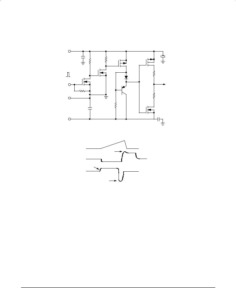
Table 1. Inductive Load Switching Drive Circuit
+15 V |
|
|
|
|
|
|
1 μF |
|
100 |
Ω |
|
MTP8P10 |
100 μF |
150 Ω |
|
|
||||
|
|
|
|
|||
|
3 W |
|
|
|
||
|
3 W |
|
|
|
||
|
|
|
|
|
|
|
|
|
|
|
|
|
MTP8P10 |
MPF930 |
|
|
|
|
MUR105 |
RB1 |
|
|
|
|
|
Iout |
|
+10 V |
MPF930 |
|
|
|
||
|
|
|
|
|
|
A |
50 Ω |
|
|
|
|
MJE210 |
RB2 |
|
|
|
|
|
||
|
|
|
|
|
|
|
COMMON |
|
|
|
150 Ω |
|
MTP12N10 |
|
|
|
|
|
||
|
μ |
|
|
|
|
|
|
F |
|
3 W |
|
|
|
|
500 |
|
|
|
|
|
|
|
|
|
|
|
1 μF |
±Voff
|
|
IC PEAK |
|
VCE PEAK |
|
VCE |
|
|
|
IB1 |
|
IB |
|
|
|
IB2 |
|
V(BR)CEO(sus) |
Inductive Switching |
RBSOA |
L = 10 mH |
L = 200 μH |
L = 500 μH |
RB2 = ∞ |
RB2 = 0 |
RB2 = 0 |
VCC = 20 Volts |
VCC = 15 Volts |
VCC = 15 Volts |
IC(pk) = 100 mA |
RB1 selected for desired IB1 |
RB1 selected for desired IB1 |
8 |
Motorola Bipolar Power Transistor Device Data |
MJE18204 MJF18204
TYPICAL THERMAL RESPONSE (IB1 = IB2 FOR ALL CURVES)
|
|
1 |
|
|
|
|
|
|
TRANSIENT THERMAL RESISTANCE |
|
|
D = 0.5 |
|
|
|
|
|
(NORMALIZED) |
|
0.2 |
|
|
|
|
|
|
|
0.1 |
|
|
P(pk) |
RθJC(t) = r(t) RθJC |
|
||
0.1 |
|
|
|
|
||||
0.05 |
|
|
|
RθJC = 1.65°C/W MAX |
|
|||
|
0.02 |
|
|
|
D CURVES APPLY FOR POWER |
|
||
|
|
|
|
PULSE TRAIN SHOWN |
|
|||
|
|
|
|
t1 |
|
|||
|
|
|
|
READ TIME AT t1 |
|
|||
|
|
|
|
t2 |
TJ(pk) ± TC = P(pk) RθJC(t) |
|
||
|
SINGLE PULSE |
|
|
DUTY CYCLE, D = t1/t2 |
|
|||
r(t), |
|
|
|
|
|
|
||
|
|
0.01 |
|
|
|
|
|
|
|
|
0.01 |
0.1 |
1 |
10 |
100 |
1000 |
|
t, TIME (ms)
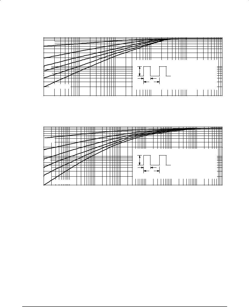
Figure 22. Typical Thermal Response (ZθJC(t)) for MJE18204
|
|
1 |
|
|
|
|
|
|
|
TRANSIENT THERMAL RESISTANCE |
|
D = 0.5 |
|
|
|
|
|
|
|
(NORMALIZED) |
0.2 |
|
|
|
P(pk) |
|
RθJC(t) = r(t) RθJC |
|
|
0.1 |
|
|
|
|
|
||||
|
|
|
|
|
° |
|
|||
0.1 |
|
|
|
|
|
RθJC = 3.55 C/W MAX |
|
||
|
|
|
|
|
D CURVES APPLY FOR POWER |
|
|||
0.05 |
|
|
|
t1 |
|
PULSE TRAIN SHOWN |
|
||
|
|
|
t2 |
READ TIME AT t1 |
|
||||
|
|
|
|
|
TJ(pk) ± TC = P(pk) RθJC(t) |
|
|||
0.02 |
|
|
|
DUTY CYCLE, D = t1/t2 |
|
||||
r(t), |
|
|
|
|
|
|
|||
|
SINGLE PULSE |
|
|
|
|
|
|
||
|
|
|
|
|
|
|
|
||
|
|
0.01 |
|
|
|
|
|
|
|
|
|
0.01 |
0.1 |
1 |
10 |
100 |
1000 |
10000 |
100000 |
t, TIME (ms)
Figure 23. Typical Thermal Response (ZθJC(t)) for MJF18204
Motorola Bipolar Power Transistor Device Data |
9 |
MJE18204 |
MJF18204 |
|
|
|
|
|
|
|
|
|
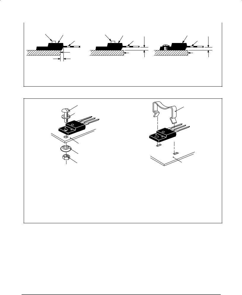
TEST CONDITIONS FOR ISOLATION TESTS* |
|
|
||
|
|
|
|
|
|
|
|
|
|
MOUNTED |
|
MOUNTED |
|
MOUNTED |
|
|
CLIP |
FULLY ISOLATED |
CLIP |
FULLY ISOLATED |
0.107″ MIN |
FULLY ISOLATED |
0.107″ MIN |
|
PACKAGE |
PACKAGE |
PACKAGE |
||||
|
|
|
|||||
LEADS |
LEADS |
HEATSINK |
HEATSINK |
0.110″ MIN |
|
LEADS
HEATSINK |
Figure 24. Screw or Clip Mounting Position for Isolation Test Number 1
Figure 25. Clip Mounting Position
for Isolation Test Number 2
Figure 26. Screw Mounting Position
for Isolation Test Number 3
* Measurement made between leads and heatsink with all leads shorted together
MOUNTING INFORMATION**
4±40 SCREW |
CLIP |
PLAIN WASHER
HEATSINK |
|
COMPRESSION WASHER |
|
NUT |
HEATSINK |
|
|
Figure 27a. Screw±Mounted |
Figure 27b. Clip±Mounted |
Figure 27. Typical Mounting Techniques
for Isolated Package
Laboratory tests on a limited number of samples indicate, when using the screw and compression washer mounting technique, a screw torque of 6 to 8 in . lbs is sufficient to provide maximum power dissipation capability. The compression washer helps to maintain a constant pressure on the package over time and during large temperature excursions.
Destructive laboratory tests show that using a hex head 4±40 screw, without washers, and applying a torque in excess of 20 in . lbs will cause the plastic to crack around the mounting hole, resulting in a loss of isolation capability.
Additional tests on slotted 4±40 screws indicate that the screw slot fails between 15 to 20 in . lbs without adversely affecting the package. However, in order to positively ensure the package integrity of the fully isolated device, Motorola does not recommend exceeding 10 in . lbs of mounting torque under any mounting conditions.
** For more information about mounting power semiconductors see Application Note AN1040.
10 |
Motorola Bipolar Power Transistor Device Data |