Материал: DS1621

DS1621
measurement will be completed and the DS1621 will remain idle until a Start Convert T is issued to resume continuous operation.
DS1621 COMMAND SET Table 3
|
|
|
2-WIRE BUS DATA |
|
|
|
|
AFTER ISSUING |
|
INSTRUCTION |
DESCRIPTION |
PROTOCOL |
PROTOCOL |
NOTES |
TEMPERATURE CONVERSION COMMANDS
Read Temperature Read last converted temperature AAh <read 2 bytes data> value from temperature register.
Read Counter |
Reads value of count remaining |
A8h |
<read data> |
|
|
from counter. |
|
|
|
Read Slope |
Reads value of the slope |
A9h |
<read data> |
|
|
accumulator. |
|
|
|
Start Convert T |
Initiates temperature |
EEh |
idle |
1 |
|
conversion. |
|
|
|
Stop Convert T |
Halts temperature conversion. |
22h |
idle |
1 |
|
THERMOSTAT COMMANDS |
|
|
|
Access TH |
Reads or writes high |
A1h |
<write data> |
2 |
|
temperature limit value into TH |
|
|
|
|
register. |
|
|
|
Access TL |
Reads or writes low |
A2h |
<write data> |
2 |
|
temperature limit value into TL |
|
|
|
|
register. |
|
|
|
Access Config |
Reads or writes configuration |
ACh |
<write data> |
2 |
|
data to configuration register. |
|
|
|
NOTES:
1.In continuous conversion mode a Stop Convert T command will halt continuous conversion. To restart the Start Convert T command must be issued. In one–shot mode a Start Convert T command must be issued for every temperature reading desired.
2.Writing to the E2 typically requires 10ms at room temperature. After issuing a write command, no further writes should be requested for at least 10 ms.
11 of 16 |
102299 |

DS1621
MEMORY FUNCTION EXAMPLE
Example: Bus master sets up DS1621 for continuous conversion and thermostatic function.
BUS MASTER |
DS1621 |
DATA (MSB |
|
|
|
MODE |
MODE |
FIRST) |
COMMENTS |
||
TX |
RX |
START |
Bus Master initiates a START condition. |
||
TX |
RX |
<address,0> |
Bus Master sends DS1621 address; R/ |
|
= 0. |
W |
|||||
RX |
TX |
ACK |
DS1621 generates acknowledge bit. |
||
TX |
RX |
ACh |
Bus Master sends Access Config command protocol. |
||
RX |
TX |
ACK |
DS1621 generates acknowledge bit. |
||
TX |
RX |
02h |
Bus Master sets up DS1621 for output polarity active |
||
|
|
|
high, continuous conversion. |
||
RX |
TX |
ACK |
DS1621 generates acknowledge bit. |
||
TX |
RX |
START |
Bus Master generates a repeated START condition. |
||
TX |
RX |
<address,0> |
Bus Master sends DS1621 address; R/ |
|
= 0. |
W |
|||||
RX |
TX |
ACK |
DS1621 generates acknowledge bit. |
||
TX |
RX |
A1h |
Bus Master sends Access TH command. |
||
RX |
TX |
ACK |
DS1621 generates acknowledge bit. |
||
TX |
RX |
28h |
Bus Master sends first byte of data for TH limit of |
||
|
|
|
+40°C. |
||
RX |
TX |
ACK |
DS1621 generates acknowledge bit. |
||
TX |
RX |
00h |
Bus Master sends second byte of data for TH limit of |
||
|
|
|
+40°C. |
||
RX |
TX |
ACK |
DS1621 generates acknowledge bit. |
||
TX |
RX |
START |
Bus Master generates a repeated START condition. |
||
TX |
RX |
<address,0> |
Bus Master sends DS1621 address; R/ |
|
= 0. |
W |
|||||
RX |
TX |
ACK |
DS1621 generates acknowledge bit. |
||
TX |
RX |
A2h |
Bus Master sends Access TL command. |
||
RX |
TX |
ACK |
DS1621 generates acknowledge bit. |
||
TX |
RX |
0Ah |
Bus Master sends first byte of data for TL limit of |
||
|
|
|
+10°C. |
||
RX |
TX |
ACK |
DS1621 generates acknowledge bit. |
||
TX |
RX |
00h |
Bus Master sends second byte of data for TL limit of |
||
|
|
|
+10°C. |
||
RX |
TX |
ACK |
DS1621 generates acknowledge bit. |
||
TX |
RX |
START |
Bus Master generates a repeated START condition. |
||
TX |
RX |
<address,0> |
Bus Master sends DS1621 address; R/ |
|
= 0. |
W |
|||||
RX |
TX |
ACK |
DS1621 generates acknowledge bit. |
||
TX |
RX |
EEh |
Bus Master sends Start Convert T command protocol. |
||
RX |
TX |
ACK |
DS1621 generates acknowledge bit. |
||
TX |
RX |
STOP |
Bus Master initiates STOP condition. |
||
12 of 16 |
102299 |

DS1621
ABSOLUTE MAXIMUM RATINGS*
Voltage on Any Pin Relative to Ground |
–0.5V to +7.0V |
Operating Temperature |
–55°C to +125°C |
Storage Temperature |
–55°C to +125°C |
Soldering Temperature |
260°C for 10 seconds |
*This is a stress rating only and functional operation of the device at these or any other conditions above those indicated in the operation sections of this specification is not implied. Exposure to absolute maximum rating conditions for extended periods of time may affect reliability.
RECOMMENDED DC OPERATING CONDITIONS
PARAMETER |
SYMBOL |
MIN |
TYP |
MAX |
UNITS |
NOTES |
Supply Voltage |
VDD |
2.7 |
|
5.5 |
V |
1 |
DC ELECTRICAL CHARACTERISTICS |
(-55°C to +125°C; VDD=2.7V to 5.5V) |
||||||
PARAMETER |
SYMBOL |
CONDITION |
MIN |
TYP |
MAX |
UNITS |
NOTES |
Thermometer Error |
TERR |
0°C to 70°C |
|
|
±½ |
°C |
|
|
|
-55°C to + 0°C |
|
|
|
|
11 |
|
|
and |
|
See Typical Curve |
|
|
|
|
|
70°C to 125°C |
|
|
|
|
|
Low Level Input |
VIL |
|
0.5 |
|
0.3 VDD |
V |
|
Voltage |
|
|
|
|
|
|
|
High Level Input |
VIH |
|
0.7 VDD |
|
VDD+0.5 |
V |
|
Voltage |
|
|
|
|
|
|
|
Pulse width of |
|
|
|
|
|
|
|
spikes which must |
tSP |
Fast Mode |
0 |
|
50 |
ns |
|
be suppressed by |
|
|
|
|
|
|
|
the input filter |
|
|
|
|
|
|
|
Low Level Output |
VOL1 |
3 mA Sink |
0 |
|
0.4 |
V |
|
Voltage |
|
Current |
|
|
|
|
|
|
VOL2 |
6 mA Sink |
0 |
|
0.6 |
V |
|
|
|
Current |
|
|
|
|
|
Input Current each |
|
0.4<VI/O<0.9VDD |
-10 |
|
10 |
µA |
2 |
I/O Pin |
|
|
|
|
|
|
|
I/O Capacitance |
CI/O |
|
|
|
10 |
pF |
|
|
|
Temperature |
|
|
|
|
|
|
|
Conversion |
|
|
1000 |
|
|
Active Supply |
ICC |
E2 Write |
|
|
400 |
µA |
3, 4 |
Current |
|
Communi- |
|
|
100 |
|
|
|
|
cation Only |
|
|
|
|
|
Standby Supply |
ISTBY |
|
|
|
1 |
µA |
3, 4 |
Current |
|
|
|
|
|
|
|
Thermostat Output |
VOH |
1 mA Source |
2.4 |
|
|
V |
|
(TOUT) Output |
VOL |
4 mA Sink |
|
|
0.4 |
V |
|
Voltage |
|
|
|
|
|
|
|
13 of 16 |
102299 |
|
|
|
|
|
|
|
|
DS1621 |
|
|
AC ELECTRICAL CHARACTERISTICS |
(-55°C to +125°C; VDD=2.7V to 5.5V) |
|
||||||
|
PARAMETER |
SYMBOL |
CONDITION |
MIN |
TYP |
MAX |
UNITS |
NOTES |
|
|
Temperature |
TTC |
|
|
0.4 |
1 |
s |
|
|
|
Conversion Time |
|
|
|
|
|
|
|
|
|
NV Write Cycle |
tWR |
0°C to 70°C |
|
10 |
50 |
ms |
10 |
|
|
Time |
|
|
|
|
|
|
|
|
|
SCL Clock |
fSCL |
Fast Mode |
0 |
|
400 |
KHz |
|
|
|
Frequency |
|
Standard Mode |
0 |
|
100 |
|
|
|
|
Bus Free Time |
tBUF |
Fast Mode |
1.3 |
|
|
µs |
|
|
|
Between a STOP |
|
Standard Mode |
4.7 |
|
|
|
|
|
|
and START |
|
|
|
|
|
|
|
|
|
Condition |
|
|
|
|
|
|
|
|
|
Hold Time |
tHD:STA |
Fast Mode |
0.6 |
|
|
µs |
5 |
|
|
(Repeated) START |
|
Standard Mode |
4.0 |
|
|
|
|
|
|
Condition |
|
|
|
|
|
|
|
|
|
Low Period of SCL |
TLOW |
Fast Mode |
1.3 |
|
|
µs |
|
|
|
Clock |
|
Standard Mode |
4.7 |
|
|
|
|
|
|
High Period of SCL |
THIGH |
Fast Mode |
0.6 |
|
|
µs |
|
|
|
Clock |
|
Standard Mode |
4.0 |
|
|
|
|
|
|
Setup Time for a |
tSU:STA |
Fast Mode |
0.6 |
|
|
µs |
|
|
|
Repeated START |
|
Standard Mode |
4.7 |
|
|
|
|
|
|
Condition |
|
|
|
|
|
|
|
|
|
Data Hold Time |
tHD:DAT |
Fast Mode |
0 |
|
0.9 |
µs |
6, 7 |
|
|
|
|
Standard Mode |
0 |
|
|
|
|
|
|
Data Setup Time |
tSU:DAT |
Fast Mode |
100 |
|
|
ns |
8 |
|
|
|
|
Standard Mode |
250 |
|
|
|
|
|
|
Rise Time of Both |
tR |
Fast Mode |
20+0.1CB |
|
300 |
ns |
9 |
|
|
SDA and SCL |
|
Standard Mode |
|
|
1000 |
|
|
|
|
Signals |
|
|
|
|
|
|
|
|
|
Fall Time of both |
tF |
Fast Mode |
20+0.1CB |
|
300 |
ns |
9 |
|
|
SDA and SCL |
|
Standard Mode |
|
|
300 |
|
|
|
|
Signals |
|
|
|
|
|
|
|
|
|
Setup time for |
tSU:STO |
Fast Mode |
0.6 |
|
|
µs |
|
|
|
STOP Condition |
|
Standard Mode |
4.0 |
|
|
|
|
|
|
Capacitative Load |
Cb |
|
|
|
400 |
pF |
|
|
|
for each Bus Line |
|
|
|
|
|
|
|
|
All values referred to VIH=0.9 VDD and VIL=0.1 VDD.
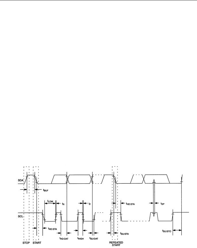
AC ELECTRICAL CHARACTERISTICS |
(-55°C to +125°C; VDD=2.7V to 5.5V) |
|||||
PARAMETER |
SYMBOL |
MIN |
TYP |
MAX |
UNITS |
NOTES |
Input Capacitance |
CI |
|
5 |
|
pF |
|
14 of 16 |
102299 |
DS1621
NOTES:
1.All voltages are referenced to ground.
2.I/O pins of fast mode devices must not obstruct the SDA and SCL lines if VDD is switched off.
3.ICC specified with TOUT pin open.
4.ICC specified with VCC at 5.0V and SDA, SCL = 5.0V, 0°C to 70°C.
5.After this period, the first clock pulse is generated.
6.A device must internally provide a hold time of at least 300 ns for the SDA signal (referred to the VIH MIN of the SCL signal) in order to bridge the undefined region of the falling edge of SCL.
7.The maximum tHD:DAT has only to be met if the device does not stretch the LOW period (tLOW) of the SCL signal.
8.A fast mode device can be used in a standard mode system, but the requirement tSU:DAT >250 ns must then be met. This will automatically be the case if the device does not stretch the LOW period of the SCL signal. If such a device does stretch the LOW period of the SCL signal, it must output the next data bit to the SDA line tRMAX+tSU:DAT = 1000+250 = 1250 ns before the SCL line is released.
9.Cb – total capacitance of one bus line in pF.
10.Writing to the nonvolatile memory should only take place in the 0°C to 70°C temperature range.
11.See typical curve for specification limits outside 0°C to 70°C range. Thermometer error reflects sensor accuracy as tested during calibration.
TIMING DIAGRAM
15 of 16 |
102299 |