Материал: MJW16212
MJW16212 |
|
|
|
|
|
|
|
||
s) |
15 |
|
|
|
|
|
|
|
1500 |
|
|
|
|
|
|
|
|
|
|
STORAGE TIME (μ |
10 |
|
|
|
|
|
|
RESISTIVE FALL TIME ( μs) |
1000 |
7 |
|
|
|
|
|
|
700 |
||
5 |
|
|
|
|
IB2 = IB1 |
500 |
|||
|
|
|
|
|
|
||||
3 |
|
|
|
|
|
|
300 |
||
|
|
|
|
|
|
|
|
||
RESISTIVE, |
2 |
βf = 5 |
|
|
I |
= 2 (I |
) |
, |
200 |
|
|
f |
|||||||
|
|
|
B2 |
B1 |
|
t |
|
||
s |
|
TJ = 25°C |
|
|
|
|
|
|
|
t |
|
|
|
|
|
|
|
|
|
|
|
|
|
|
|
|
|
|
|
|
1 |
2 |
3 |
5 |
7 |
10 |
|
15 |
100 |
|
1 |
|
|
||||||
|
|
|
IC, COLLECTOR CURRENT (A) |
|
|
|
|||
|
|
|
IB2 = IB1 |
|
|
|
|
|
|
|
IB2 = 2 (IB1) |
|
|
|
|
βf = 5 |
|
|
|
|
|
|
TJ = 25°C |
|
|
|
|
1 |
2 |
3 |
5 |
7 |
10 |
15 |
IC, COLLECTOR CURRENT (A)
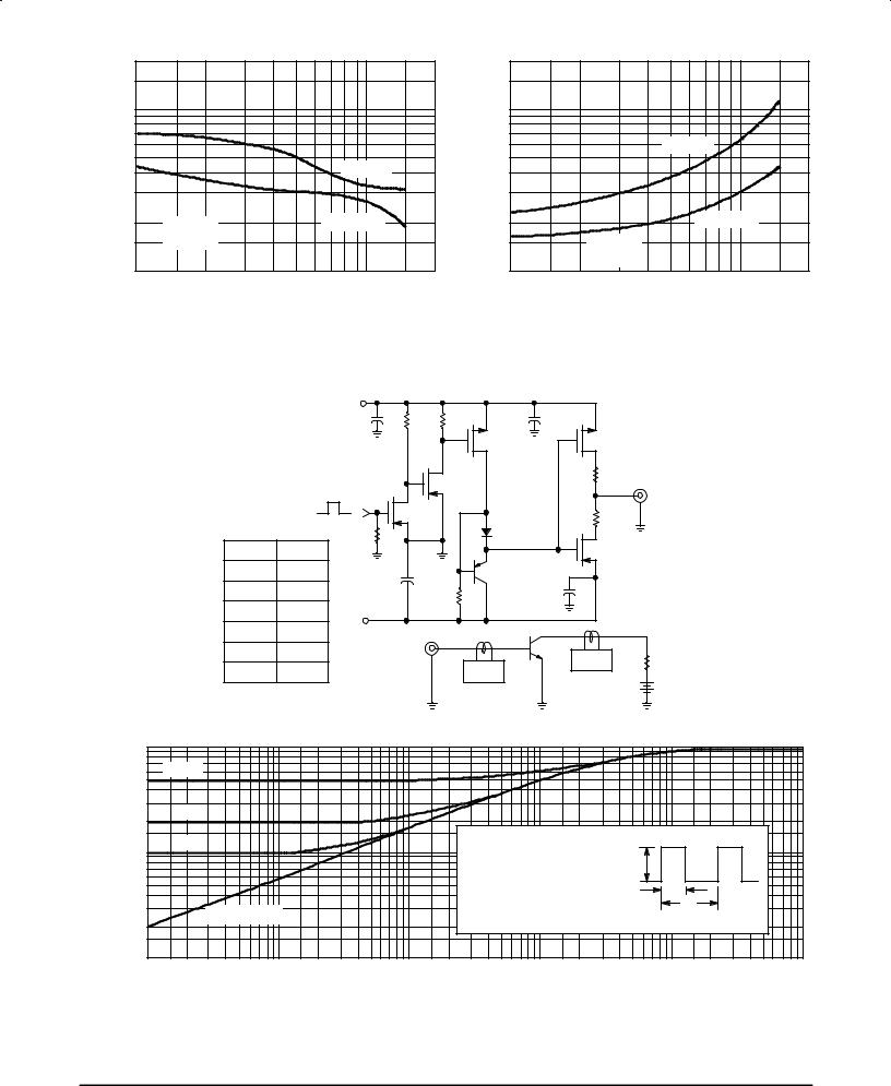
Figure 11. Typical Resistive Storage Time |
|
|
|
|
Figure 12. Typical Resistive Fall Time |
||
|
Table 3. Resistive Load Switching |
||||||
ts and tf |
+15 |
|
|
|
|
|
|
1 F |
150 |
|
100 |
|
100 μF |
|
|
|
μ |
|
Ω |
|
Ω |
|
|
|
|
|
|
|
|
MTP8P10 |
MTP8P10 |
V(off) adjusted |
|
|
|
MPF930 |
|
RB1 |
|
to give specified |
|
|
|
|
|
||
off drive |
+10 V |
|
|
A |
|
|
|
MPF930 |
|
|
|
|
|
|
RB2 |
|
|
|
|
|
|
|
|
|
|
50 Ω |
|
MUR105 |
|
VCC |
250 V |
|
|
MTP12N10 |
|
RL |
28 Ω |
500 |
μF |
MJE210 |
|
IC |
5.5 A |
|
|
||
|
150 Ω |
1 μF |
|
||
IB1 |
1.1 A |
Voff |
|
|
|
IB2 |
Per Spec |
|
|
|
|
|
|
|
|
||
RB1 |
3.3 Ω |
|
A |
T.U.T. |
|
|
|
*IC |
RL |
||
RB2 |
|
|
|
||
Per Spec |
|
|
*IB |
|
|
|
|
|
|
VCC |
|
|
|
1 |
|
|
|
|
|
|
|
0.5 |
D = 0.5 |
|
|
|
|
|
RESISTANCE (NORMALIZED) |
|
|
|
|
|
|
r(t), TRANSIENT THERMAL |
0.2 |
0.2 |
|
|
|
|
|
|
|
|
|
|
|||
0.1 |
0.1 |
|
RθJC(t) = r(t) RθJC |
P(pk) |
|
||
|
|
RθJC = 0.7°C/W MAX |
|
|
|||
0.05 |
|
|
D CURVES APPLY FOR POWER |
|
|
||
|
|
PULSE TRAIN SHOWN |
t1 |
|
|||
|
|
|
READ TIME AT t1 |
|
|||
|
|
|
t |
|
|||
|
SINGLE PULSE |
|
TJ(pk) ± TC = P(pk) RθJC(t) |
2 |
|
||
|
|
DUTY CYCLE, D = t1/t2 |
|
||||
|
|
|
|
|
|||
|
|
|
|
|
|
|
|
|
|
0.01 |
|
|
100 |
1000 |
10000 |
|
|
0.1 |
1 |
10 |
t, TIME (ms)
Figure 13. Thermal Response
3±6 |
Motorola Bipolar Power Transistor Device Data |
EMITTER±BASE TURN±OFF ENERGY, EB(off)
Emitter±base turn±off energy is a new specification included on the SCANSWITCH data sheets. Typical techniques for driving horizontal outputs rely on a pulse transformer to supply forward base current, and a turnoff network that includes a series base inductor to limit the rate of transition from forward to reverse. An alternate drive scheme has been used to characterize the SCANSWITCH series of devices (see Figure 2). This circuit ramps the base drive to eliminate the heavy overdrive at the beginning of the collector current ramp and underdrive just prior to turn±off observed in typical drive topologies. This high performance
MJW16212
drive has two additional important advantages. First, the configuration of T1 allows Lb to be placed outside the path of forward base current making it unnecessary to expend energy to reverse the current flow as in a series based inductor. Second, there is no base resistor to limit forward base current and hence no power loss associated with setting the value of the forward base current. The ramp generating process stores rather than dissipates energy. Tailoring the amount of
energy stored in T1 to the amount of energy, EB(off), that is required to turn the output transistor off results in essentially
lossless operation. [Note: B+ and the primary inductance of T1 (LP) are chosen such that 1/2LPlb2 = EB(off).]
TEST CONDITIONS FOR ISOLATION TESTS* (MJF16212 ONLY)
MOUNTED
FULLY ISOLATED
PACKAGE
LEADS
HEATSINK |
0.110º MIN |
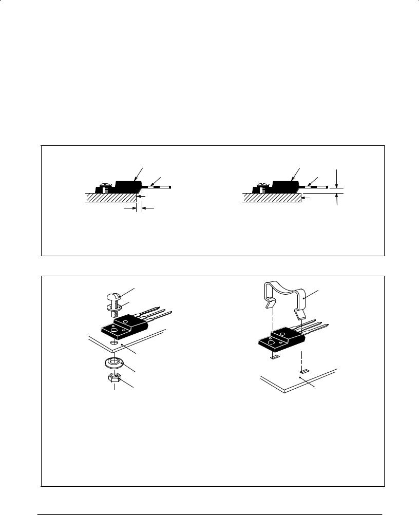
Figure 14. Screw or Clip Mounting Position for Isolation Test Number 1
MOUNTED |
|
FULLY ISOLATED |
|
PACKAGE |
0.099º MIN |
|
|
|
LEADS |
HEATSINK |
Figure 15. Screw or Clip Mounting Position for Isolation Test Number 2
* Measurement made between leads and heatsink with all leads shorted together
MOUNTING INFORMATION** (MJF16212 ONLY)
4±40 SCREW |
CLIP |
PLAIN WASHER
HEATSINK
COMPRESSION WASHER
NUT |
HEATSINK |
|
Figure 16a. Screw±Mounted Figure 16b. Clip±Mounted
Figure 16. Typical Mounting Techniques*
Laboratory tests on a limited number of samples indicate, when using the screw and compression washer mounting technique, a screw torque of 6 to 8 in . lbs is sufficient to provide maximum power dissipation capability. The compression washer helps to maintain a constant pressure on the package over time and during large temperature excursions.
Destructive laboratory tests show that using a hex head 4-40 screw, without washers, and applying a torque in excess of 20 in . lbs will cause the plastic to crack around the mounting hole, resulting in a loss of isolation capability.
Additional tests on slotted 4-40 screws indicate that the screw slot fails between 15 to 20 in . lbs without adversely affecting the package. However, in order to positively ensure the package integrity of the fully isolated device, Motorola does not recommend exceeding 10 in . lbs of mounting torque under any mounting conditions.
** For more information about mounting power semiconductors see Application Note AN1040.
Motorola Bipolar Power Transistor Device Data |
3±7 |
MJW16212
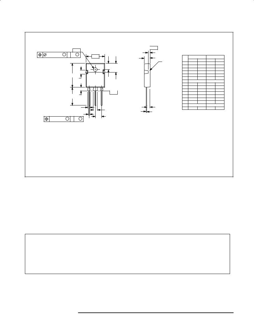
PACKAGE DIMENSIONS
|
|
|
|
|
|
NOTES: |
|
|
|
|
|
|
|
|
|
|
±T± |
1. |
DIMENSIONING AND TOLERANCING PER ANSI |
||||
|
±Q± |
|
|
Y14.5M, 1982. |
|
|
|
||||
|
|
|
E |
|
|
|
|||||
0.25 (0.010) M T |
B |
M |
|
|
2. |
CONTROLLING DIMENSION: MILLIMETER. |
|||||
±B± |
|
C |
|
|
MILLIMETERS |
INCHES |
|||||
|
|
|
|
|
|
||||||
|
|
|
|
|
|
|
|||||
|
|
|
|
|
|
4 |
DIM |
MIN |
MAX |
MIN |
MAX |
|
|
|
|
|
|
A |
20.40 |
20.90 |
0.803 |
0.823 |
|
|
|
|
|
U |
|
|
|||||
|
|
|
|
L |
|
B |
15.44 |
15.95 |
0.608 |
0.628 |
|
|
|
|
|
|
|
C |
4.70 |
5.21 |
0.185 |
0.205 |
|
|
|
|
|
|
|
|
|||||
|
A |
|
|
|
|
|
D |
1.09 |
1.30 |
0.043 |
0.051 |
|
R |
|
|
|
|
E |
1.50 |
1.63 |
0.059 |
0.064 |
|
|
|
|
|
|
|
F |
1.80 |
2.18 |
0.071 |
0.086 |
|
|
|
1 |
2 |
3 |
|
|
G |
5.45 BSC |
0.215 BSC |
||
|
|
|
|
H |
2.56 |
2.87 |
0.101 |
0.113 |
|||
|
|
|
|
|
|
|
J |
0.48 |
0.68 |
0.019 |
0.027 |
|
|
|
|
|
±Y± |
|
K |
15.57 |
16.08 |
0.613 |
0.633 |
|
K |
P |
|
|
|
L |
7.26 |
7.50 |
0.286 |
0.295 |
|
|
|
|
|
|
P |
3.10 |
3.38 |
0.122 |
0.133 |
||
|
|
|
|
|
|
|
Q |
3.50 |
3.70 |
0.138 |
0.145 |
|
|
|
|
|
|
|
R |
3.30 |
3.80 |
0.130 |
0.150 |
|
|
F |
|
|
H |
|
U |
5.30 BSC |
0.209 BSC |
||
|
|
|
V |
|
V |
3.05 |
3.40 |
0.120 |
0.134 |
||
|
|
|
|
J |
|
STYLE 3: |
|
|
|
||
|
|
D |
|
|
|
|
|
|
|||
|
|
|
|
|
|
|
|
|
|||
|
|
G |
|
|
|
PIN 1. BASE |
|
|
|
||
|
|
|
|
|
|
|
|
|
|||
0.25 (0.010) M |
Y |
Q S |
|
|
|
|
2. COLLECTOR |
|
|
||
|
|
|
|
|
|
|
|||||
|
|
|
|
|
|
|
|
3. EMITTER |
|
|
|
|
|
|
|
|
|
|
|
4. COLLECTOR |
|
|
|
CASE 340F±03
TO±247AE
ISSUE E
Motorola reserves the right to make changes without further notice to any products herein. Motorola makes no warranty, representation or guarantee regarding the suitability of its products for any particular purpose, nor does Motorola assume any liability arising out of the application or use of any product or circuit, and specifically disclaims any and all liability, including without limitation consequential or incidental damages. ªTypicalº parameters can and do vary in different applications. All operating parameters, including ªTypicalsº must be validated for each customer application by customer's technical experts. Motorola does not convey any license under its patent rights nor the rights of others. Motorola products are not designed, intended, or authorized for use as components in systems intended for surgical implant into the body, or other applications intended to support or sustain life, or for any other application in which the failure of the Motorola product could create a situation where personal injury or death may occur. Should Buyer purchase or use Motorola products for any such unintended or unauthorized application, Buyer shall indemnify and hold Motorola and its officers, employees, subsidiaries, affiliates, and distributors harmless against all claims, costs, damages, and expenses, and reasonable attorney fees arising out of, directly or indirectly, any claim of personal injury or death associated with such unintended or unauthorized use, even if such claim alleges that Motorola was negligent regarding the design or manufacture of the part. Motorola and  are registered trademarks of Motorola, Inc. Motorola, Inc. is an Equal Opportunity/Affirmative Action Employer.
How to reach us: |
|
USA / EUROPE: Motorola Literature Distribution; |
JAPAN: Nippon Motorola Ltd.; Tatsumi±SPD±JLDC, Toshikatsu Otsuki, |
P.O. Box 20912; Phoenix, Arizona 85036. 1±800±441±2447 |
6F Seibu±Butsuryu±Center, 3±14±2 Tatsumi Koto±Ku, Tokyo 135, Japan. 03±3521±8315 |
MFAX: RMFAX0@email.sps.mot.com ± TOUCHTONE (602) 244±6609 HONG KONG: Motorola Semiconductors H.K. Ltd.; 8B Tai Ping Industrial Park, |
|
INTERNET: http://Design±NET.com |
51 Ting Kok Road, Tai Po, N.T., Hong Kong. 852±26629298 |
◊ MJW16212/D
*MJW16212/D*