Материал: FSDM311_FAIR

FSDM311
Electrical Characteristics (Control Part) (Continued)
(Ta=25° C unless otherwise specified)
Parameter |
Symbol |
Condition |
|
Min. |
Typ. |
Max. |
Unit |
||
|
|
|
|
|
|
|
|
|
|
UVLO SECTION |
|
|
|
|
|
|
|
|
|
Start Threshold Voltage |
VSTART |
VFB=GND |
|
|
|
8 |
9 |
10 |
V |
|
|
|
|
|
|
|
|
|
|
Stop Threshold Voltage |
VSTOP |
VFB=GND |
|
|
|
6 |
7 |
8 |
V |
|
|
|
|
|
|
|
|
|
|
OSCILLATOR SECTION |
|
|
|
|
|
|
|
|
|
|
|
|
|
|
|
|
|
|
|
Initial Accuracy |
FOSC |
|
|
|
|
61 |
67 |
73 |
kHz |
Frequency Change With Temperature (2) |
∆ F/∆ T |
-25° C ≤ Ta ≤ |
+85° C |
|
- |
± 5 |
± 10 |
% |
|
Maximum Duty Cycle |
Dmax |
|
|
|
|
60 |
67 |
74 |
% |
|
|
|
|
|
|
|
|
|
|
FEEDBACK SECTION |
|
|
|
|
|
|
|
|
|
|
|
|
|
|
|
|
|
|
|
Feedback Source Current |
IFB |
Ta=25° C, 0V ≤ |
Vfb ≤ |
3V |
0.35 |
0.40 |
0.45 |
mA |
|
Shutdown Feedback Voltage |
VSD |
|
|
|
|
4.0 |
4.5 |
5.0 |
V |
|
|
|
|
|
|
|
|
|
|
Shutdown Delay Current |
IDELAY |
Ta=25° C, 3V ≤ |
Vfb ≤ |
VSD |
4 |
5 |
6 |
A |
|
|
|
|
|
|
|
|
|
|
|
BURST MODE SECTION |
|
|
|
|
|
|
|
|
|
|
|
|
|
|
|
|
|
|
|
|
VBURH |
|
|
|
|
0.6 |
0.70 |
0.8 |
V |
Burst Mode Voltage |
|
Tj = 25° C |
|
|
|
|
|
|
|
VBURL |
|
|
|
0.45 |
0.55 |
0.65 |
V |
||
|
|
|
|
|
|
|
|
|
|
|
Hysteresis |
|
|
|
|
- |
150 |
- |
mV |
|
|
|
|
|
|
|
|
|
|
REFERENCE SECTION |
|
|
|
|
|
|
|
|
|
Output Voltage (1) |
Vref |
Ta=25° C |
|
|
|
4.20 |
4.50 |
4.80 |
V |
Temperature Stability (1)(2) |
Vref/∆ T |
-25° C ≤ Ta ≤ |
+85° C |
|
- |
0.3 |
0.6 |
mV/° C |
|
CURRENT LIMIT(SELF-PROTECTION)SECTION |
|
|
|
|
|
|
|
|
|
|
|
|
|
|
|
|
|
|
|
Peak Current Limit |
IOVER |
|
|
|
|
0.475 |
0.55 |
0.625 |
A |
|
|
|
|
|
|
|
|
|
|
SOFT START SECTION |
|
|
|
|
|
|
|
|
|
|
|
|
|
|
|
|
|
|
|
Soft Start Time |
TSOFT |
|
|
|
|
10 |
15 |
20 |
ms |
|
|
|
|
|
|
|
|
|
|
PROTECTION SECTION |
|
|
|
|
|
|
|
|
|
|
|
|
|
|
|
|
|
|
|
Thermal Shutdown Temperature (1) |
TSD |
- |
|
|
|
125 |
145 |
- |
° C |
Over Voltage Protection |
VOVP |
|
|
|
|
20 |
- |
- |
V |
|
|
|
|
|
|
|
|
|
|
TOTAL STANDBY CURRENT SECTION |
|
|
|
|
|
|
|
|
|
|
|
|
|
|
|
|
|
||
Start-up Current |
ISTR |
VCC=0V, VSTR=50V |
|
450 |
550 |
650 |
A |
||
Operating Supply Current |
IOP |
VCC ≤ 16 |
|
|
|
- |
1.5 |
3.0 |
mA |
(Control Part Only) |
|
|
|
||||||
|
|
|
|
|
|
|
|
|
|
|
|
|
|
|
|
|
|
|
|
Note:
1.These parameters, although guaranteed, are not 100% tested in production
2.These parameters, although guaranteed, are tested in EDS (wafer test) process
6

FSDM311
Comparison Between FSDH0165 and FSDM311
Function |
FSDH0165 |
FSDM311 |
FSDM311 Advantages |
|
|
|
|
Soft-Start |
not applicable |
15mS |
• Gradually increasing current limit |
|
|
|
during soft-start further reduces peak |
|
|
|
current and voltage component |
|
|
|
stresses |
|
|
|
• Eliminates external components used |
|
|
|
for soft-start in most applications |
|
|
|
• Reduces or eliminates output |
|
|
|
overshoot |
|
|
|
|
Burst Mode Operation |
not applicable |
Yes-built into |
• Improve light load efficiency |
|
|
controller |
• Reduces no-load consumption |
|
|
|
• Transformer audible noise reduction |
Drain Creepage at |
1.02mm |
3.56mm DIP |
• Greater immunity to arcing as a result |
Package |
|
3.56mm LSOP |
of build-up of dust, debris and other |
|
|
|
contaminants |
|
|
|
|
7
FSDM311
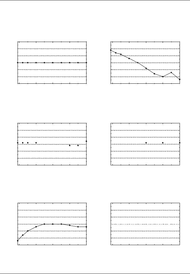
Typical Performance Characteristics
(These characteristic graphs are normalized at Ta=25° C)
Vref
1.15 |
|
|
|
|
|
1.15 |
|
|
|
|
1.10 |
|
|
|
|
|
1.10 |
|
|
|
|
1.05 |
|
|
|
|
|
1.05 |
|
|
|
|
1.00 |
|
|
|
|
Iop |
1.00 |
|
|
|
|
|
|
|
|
|
|
|
|
|
|
|
0.95 |
|
|
|
|
|
0.95 |
|
|
|
|
0.90 |
|
|
|
|
|
0.90 |
|
|
|
|
0.85 |
0 |
50 |
100 |
150 |
|
0.85 |
0 |
50 |
100 |
150 |
-50 |
|
-50 |
||||||||
|
|
Temperature('C) |
|
|
|
|
|
Temperature('C) |
|
|
Reference Voltage vs. Temp |
Operating Current vs. Temp |
Vstart
1.15
1.10
1.05
1.00 


0.95
0.90
0.85
-50 |
0 |
50 |
100 |
150 |
Temperature('C)
Start Threshold Voltage vs. Temp
Vstop
1.15
1.10
1.05
1.00


0.95
0.90
0.85
-50 |
0 |
50 |
100 |
150 |
Temperature('C)
Stop Threshold Voltage vs. Temp
|
1.15 |
|
|
|
|
|
1.10 |
|
|
|
|
|
1.05 |
|
|
|
Dmax |
Fosc |
1.00 |
|
|
|
|
|
|
|
|
|
|
|
0.95 |
|
|
|
|
|
0.90 |
|
|
|
|
|
0.85 |
0 |
50 |
100 |
150 |
|
-50 |
||||
|
|
|
Temperature('C) |
|
|
1.15
1.10
1.05
1.00


0.95
0.90
0.85
-50 |
0 |
50 |
100 |
150 |
Temperature('C)
Frequency vs. Temp |
Maximum Duty vs. Temp |
8
FSDM311
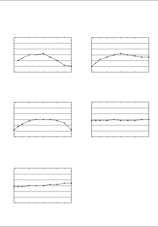
Typical Performance Characteristics (Continued)
(These characteristic graphs are normalized at Ta=25° C)
|
1.15 |
|
|
|
|
|
1.10 |
|
|
|
|
|
1.05 |
|
|
|
|
Iover |
1.00 |
|
|
|
|
|
|
|
|
|
|
|
0.95 |
|
|
|
|
|
0.90 |
|
|
|
|
|
0.85 |
0 |
50 |
100 |
150 |
|
-50 |
||||
|
|
|
Temperature('C) |
|
|
Peak Current Limit vs. Temp
|
1.15 |
|
|
|
|
|
1.10 |
|
|
|
|
|
1.05 |
|
|
|
|
Idelay |
1.00 |
|
|
|
|
|
|
|
|
|
|
|
0.95 |
|
|
|
|
|
0.90 |
|
|
|
|
|
0.85 |
0 |
50 |
100 |
150 |
|
-50 |
||||
|
|
|
Temperature('C) |
|
|
ShutDown Delay Current vs. Temp
|
1.15 |
|
|
|
|
|
1.10 |
|
|
|
|
Vovp |
1.05 |
|
|
|
|
1.00 |
|
|
|
|
|
|
|
|
|
|
|
|
0.95 |
|
|
|
|
|
0.90 |
|
|
|
|
|
0.85 |
0 |
50 |
100 |
150 |
|
-50 |
Temperature('C)
|
1.15 |
|
|
|
|
|
1.10 |
|
|
|
|
|
1.05 |
|
|
|
|
Ifb |
1.00 |
|
|
|
|
|
|
|
|
|
|
|
0.95 |
|
|
|
|
|
0.90 |
|
|
|
|
|
0.85 |
0 |
50 |
100 |
150 |
|
-50 |
||||
|
|
|
Temperature('C) |
|
|
Feedback Source Current vs. Temp
|
1.15 |
|
|
|
|
|
1.10 |
|
|
|
|
|
1.05 |
|
|
|
|
Vsd |
1.00 |
|
|
|
|
|
|
|
|
|
|
|
0.95 |
|
|
|
|
|
0.90 |
|
|
|
|
|
0.85 |
0 |
50 |
100 |
150 |
|
-50 |
||||
|
|
|
Temperature('C) |
|
|
ShutDown Feedback Voltage vs. Temp
Over Voltage Protection vs. Temp
9
FSDM311
Functional Description
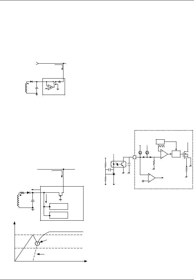
1. Startup : At startup, the internal high voltage current source supplies the internal bias and charges the external Vcc capacitor as shown in Figure 4. In the case of the FSDM311, when Vcc reaches 9V the device starts switching and the internal high voltage current source is disabled. The device continues to switch provided that Vcc does not drop below 7V. After startup the bias is supplied from the auxiliary transformer winding.
Vin,dc |
|
|
Istr |
|
Vstr |
Vcc |
L |
|
H |
9V/ |
FSDM311 |
7V |
Figure 4. Internal startup circuit
Calculating the Vcc capacitor is an important step to designing in the FSDM311. At initial start-up in the FSDM311, the stand-by maximum current is 100uA, supplying current to UVLO and Vref Block. The charging current (i) of the Vcc capacitor is equal to Istr - 100uA. After Vcc reaches the UVLO start voltage only the bias winding supplies Vcc current to device. When the bias winding voltage is not sufficient, the Vcc level decreases to the UVLO stop voltage. At this time Vcc oscillates. In order to prevent this ripple it is recommended that the Vcc capacitor be sized between 10uF and 47uF.
Vin,dc |
|
|
|
Istr |
|
|
Vstr |
|
i = Istr-max current |
|
|
i = Istr-max current |
|
J-FET |
Vcc |
|
|
max |
|
|
|
|
|
|
current |
|
|
UVLO |
|
|
Vref |
FSDM311 |
|
|
Vcc
UVLO start
Vcc must not drop to UVLO stop
UVLO stop
Auxiliary winding voltage
t
Figure 5. Charging the Vcc capacitor through Vstr
2.Feedback Control : The FSDM311 are the voltage mode devices as shown in Figure 6. Usually, an opto-coupler and KA431 type voltage reference are used to implement the feedback network. The feedback voltage is compared with an internally generated sawtooth waveform. This directly controls the duty cycle. When the KA431 reference pin voltage exceeds the internal reference voltage of 2.5V, the optocoupler LED current increase pulling down the feedback voltage and reducing the duty cycle. This will happen when the input voltage increases or the output load decreases.
3.Leading edge blanking (LEB) : When the MOSFET is turned on, there usually exists a high current spike through the MOSFET. This is caused by primary side capacitance and secondary side rectifier reverse recovery. This could cause premature termination of the switching pulse if it exceeded the over-current threshold. Therefore, the FPS employs the leading edge blanking (LEB) circuit. This circuit inhibits the over current comparator for a short time after the MOSFET is turned on.
|
|
Vcc |
OSC |
|
|
|
Vref |
||
|
|
5uA |
0.40mA |
|
Vo |
Vfb |
FB |
Gate |
|
driver |
||||
4 |
||||
|
|
|
||
|
|
Cfb |
R |
|
|
KA431 |
|
|
|
|
|
VSD |
OLP |
|
|
|
|
Figure 6. PWM and feedback circuit
4. Protection Circuit : The FSDM311 has 3self protection functions: over-load protection (OLP), thermal shutdown (TSD) and over-voltage protection. Because these protection circuits are fully integrated into the IC with no external components, system reliability is improved without cost increase. If either of these functions are triggered, the FPS starts an auto-restart cycle. Once the fault condition occurs, switching is terminated and the MOSFET remains off. This cause Vcc to fall. When Vcc reaches the UVLO stop voltage (7V), the protection is reset and the internal high voltage current source charges the Vcc capacitor. When Vcc reaches the UVLO start voltage (9V), the device attempts to resume normal operation. If the fault condition is no longer present start up will be successful. If it is still present the cycle is repeated. This is shown in Figure 7.
10