Материал: FSDM311_FAIR
www.fairchildsemi.com
FSDM311
Green Mode Fairchild Power Switch (FPSTM)
Features
•Internal Avalanche Rugged Sense FET
•Precision Fixed Operating Frequency (67kHz)
•Advanced Burst-Mode operation Consumes under 0.2W at 265Vac and no load
•Internal Start-up Switch and Soft Start
•Under Voltage Lock Out (UVLO) with Hysteresis
•Pulse by Pulse Current Limit
•Over Load Protection (OLP)
•Over Voltage Protection (OVP)
•Internal Thermal Shutdown Function (TSD)
•Secondary Side Regulation
•Auto-Restart Mode
TYPICAL POWER CAPABILITY
PRODUCT |
Open Frame |
||
|
|
||
230VAC ± 15%(1) |
85-265VAC |
||
|
|||
FSDM311 |
20W |
12W |
|
|
|
|
|
FSDM311L |
20W |
12W |
|
|
|
|
|
Table 1. Notes: 1. 230 VAC or 100/115 VAC with doubler.
Typical Circuit
Applications
•Charger & Adaptor for Mobile Phone, PDA & MP3
•Auxiliary Power for White Goods, PC, C-TV & Monitor
Description
The FSDM311 is an integrated Pulse Width Modulator (PWM) and Sense FET specially designed for high performance off-line Switch Mode Power Supplies (SMPS) with minimal external components. This device is a monolithic high voltage power switching regulator which combines an VDMOS Sense FET with a voltage mode PWM control block. The integrated PWM controller features include: a fixed oscillator, Under Voltage Lock Out (UVLO) protection, Leading Edge Blanking (LEB), optimized gate turn-on/ turn-off driver, thermal shut down protection (TSD), temperature compensated precision current sources for loop compensation and fault protection circuitry. When compared to a discrete MOSFET and controller or RCC switching converter solution, the FSDM311 reduces total component count, design size, weight and at the same time increases efficiency, productivity, and system reliability. This device is a basic platform well suited for cost effective designs of flyback converters.
AC
IN  DC OUT
Vstr |
Drain |
PWM |
|
Vfb Vcc Source
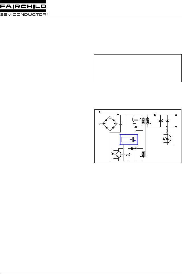
Figure 1. Typical Flyback Application using FSDM311
Rev.1.0.4
©2004 Fairchild Semiconductor Corporation
FSDM311
Internal Block Diagram
|
|
|
|
|
|
|
Vstr |
|
|
|
|
|
|
|
|
|
5 |
6,7,8 |
Drain |
Vcc |
2 |
|
|
|
|
|
L |
|
|
|
|
|
|
|
|
|
|
||
|
|
UVLO |
Voltage |
|
Internal |
|
H |
|
|
|
|
Ref |
|
Bias |
|
|
|
|
|
|
|
|
|
|
|
|
|
||
|
|
|
|
|
8.7/6.7V |
|
|
|
|
|
|
|
|
OSC |
Vck |
|
|
|
|
|
5uA |
400uA |
|
|
|
|
|
|
|
|
|
|
|
|
DRIVER |
SFET |
|
||
|
|
|
|
PWM |
|
|
|
||
|
|
|
|
S |
Q |
|
|
|
|
Vfb |
3 |
|
|
|
|
|
|
||
|
|
|
R |
|
|
|
|
||
|
|
|
|
|
|
|
|
|
|
|
|
|
S/S |
|
|
|
|
|
|
|
|
|
15mS |
|
|
|
|
|
|
|
|
|
BURST |
|
|
|
|
|
|
|
|
VBURST |
|
|
|
LEB |
|
|
|
NC |
4 |
|
|
OLP |
|
|
Iover |
|
|
|
|
Reset |
|
|
|
|
Rsense |
|
|
|
|
|
|
|
|
Vth |
|
||
|
|
|
|
S |
Q |
|
|
||
|
|
|
VSD |
|
|
|
|||
|
|
|
|
|
|
|
|||
|
|
OVP |
|
R |
|
|
|
|
|
|
|
|
|
|
|
|
|
||
|
Min.20V |
|
TSD |
|
|
|
|
|
|
|
|
|
|
A/R |
|
|
|
|
|
|
|
|
|
|
|
|
|
|
|
|
|
|
|
|
|
|
|
1 |
GND |
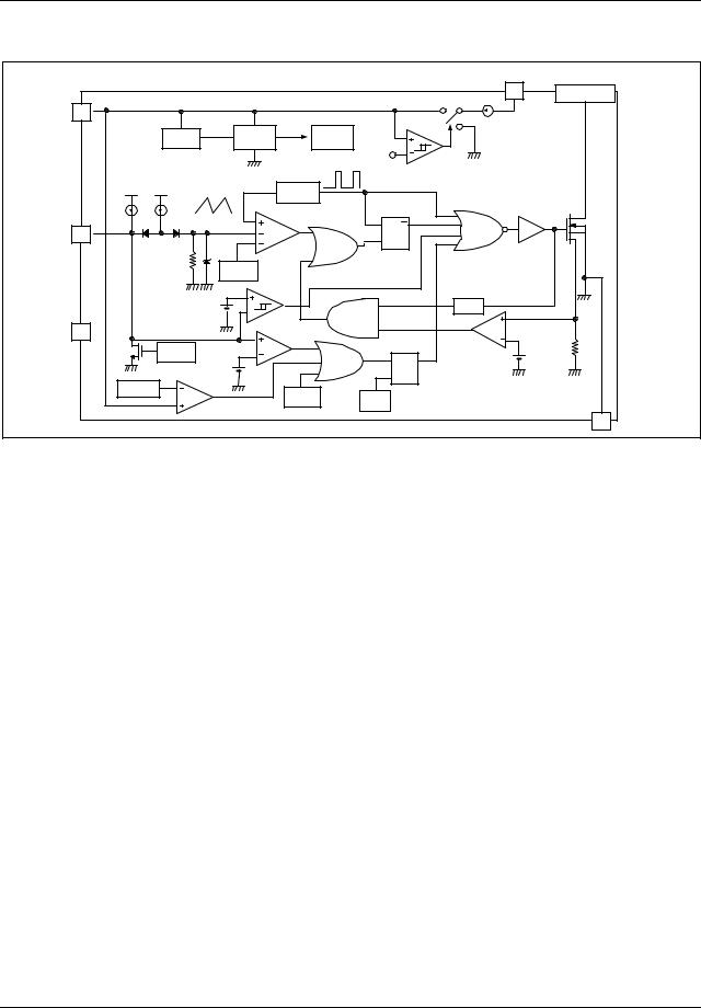
Figure 2. Functional Block Diagram of FSDM311
2

FSDM311
Pin Definitions
Pin Number |
Pin Name |
Pin Function Description |
|
1 |
GND |
Sense FET source terminal on primary side and internal control ground. |
|
|
|
|
|
|
|
Positive supply voltage input. Although connected to an auxiliary |
|
|
|
transformer winding, current is supplied from pin 8 (Vstr) via an internal |
|
2 |
Vcc |
switch during startup (see Internal Block Diagram section). It is not until Vcc |
|
|
|
reaches the UVLO upper threshold (8.7V) that the internal start-up switch |
|
|
|
opens and device power is supplied via the auxiliary transformer winding. |
|
|
|
|
|
|
|
The feedback voltage pin is the inverting input to the PWM comparator with |
|
|
|
nominal input levels between 0.5Vand 2.5V. It has a 0.40mA current source |
|
|
|
connected internally while a capacitor and opto coupler are typically |
|
|
|
connected externally. A feedback voltage of 4.5Vtriggers overload |
|
3 |
Vfb |
protection |
|
|
|
(OLP). There is a time delay while charging between 3V and 4.5V using an |
|
|
|
internal 5uA current source, which prevents false triggering under transient |
|
|
|
conditions but still allows the protection mechanism to operate under true |
|
|
|
overload conditions. |
|
|
|
The startup pin connects directly to the rectified AC line voltage source for |
|
5 |
Vstr |
FSDM311. For the FSDM311, at start up the internal switch supplies internal |
|
bias and charges an external storage capacitor placed between the Vcc pin |
|||
|
|
||
|
|
and ground. Once this reaches 9V, the internal current source is disabled. |
|
|
|
|
|
|
|
The Drain pin is designed to connect directly to the primary lead of the |
|
6, 7, 8 |
Drain |
transformer and is capable of switching a maximum of 650V. Minimizing the |
|
length of the trace connecting this pin to the transformer will decrease |
|||
|
|
||
|
|
leakage inductance. |
|
|
|
|
Pin Configuration
8DIP
8LSOP
|
|
|
|
Drain |
GND |
1 |
|
8 |
|
|
|
|
|
|
Vcc |
2 |
|
7 |
Drain |
|
|
|
|
|
Vfb |
3 |
|
6 |
Drain |
Ipk |
|
|
|
Vstr |
4 |
|
5 |
||
|
|
|
|
|
Figure 3. Pin Configuration (Top View)
3

FSDM311
Absolute Maximum Ratings
(Ta=25° C unless otherwise specified)
Parameter |
Symbol |
Value |
Unit |
|
|
|
|
Maximum Vstr Pin Voltage |
VSTR,MAX |
650 |
V |
Maximum Drain Pin Voltage |
VDRAIN,MAX |
650 |
V |
|
|
|
|
Drain-Gate Voltage (RGS=1MΩ ) |
VDGR |
650 |
V |
|
|
|
|
Gate-Source (GND) Voltage |
VGS |
± 20 |
V |
Drain Current Pulsed (1) |
IDM |
1.5 |
ADC |
Continuous Drain Current (Tc=25° C) |
ID |
0.5 |
ADC |
|
|
|
|
Continuous Drain Current (Tc=100° C) |
ID |
0.32 |
ADC |
|
|
|
|
Single Pulsed Avalanche Energy (2) |
EAS |
10 |
mJ |
Maximum Supply Voltage |
VCC,MAX |
20 |
V |
Input Voltage Range |
VFB |
− 0.3 to Vstop |
V |
|
|
|
|
Total Power Dissipation |
PD |
1.25 |
W |
|
|
|
|
Operating Junction Temperature. |
TJ |
+150 |
° C |
Operating Ambient Temperature. |
TA |
-25 to +85 |
° C |
Storage Temperature Range. |
TSTG |
-55 to +150 |
° C |
|
|
|
|
1.Repetitive rating: Pulse width limited by maximum junction temperature
2.L=24mH, starting Tj=25° C
Thermal Impedance
Parameter |
Symbol |
Value |
Unit |
|
8DIP |
|
|
|
|
|
|
|
|
|
Junction-to-Ambient Thermal |
θ JA(1) |
?(3) |
° C/W |
|
θ JA(1) |
?(4) |
° C/W |
||
|
||||
Junction-to-Case Thermal |
θ JC(2) |
|
° C/W |
Note:
1.Free standing without heatsink.
2.Measured on the GND pin close to plastic interface.
3.Soldered to 100mm2 copper clad.
4.Soldered to 300mm2 copper clad.
4

FSDM311
Electrical Characteristics (Sense FET Part)
(Ta = 25° C unless otherwise specified)
Parameter |
|
Symbol |
Condition |
Min. |
Typ. |
Max. |
Unit |
|||
|
|
|
|
|
|
|
|
|
||
Sense FET SECTION |
|
|
|
|
|
|
|
|
||
Drain-Source Breakdown Voltage |
|
BVDSS |
VGS=0V, ID=50µ A |
650 |
720 |
- |
V |
|||
|
|
|
|
|
|
|
|
|
|
|
|
|
|
|
|
VDS=Max. Rating, |
- |
- |
25 |
µ |
A |
|
|
|
|
|
VGS=0V |
|||||
Zero Gate Voltage Drain Current |
|
IDSS |
|
|
|
|
|
|||
|
VDS=0.8Max. Rating, |
- |
- |
200 |
µ |
A |
||||
|
|
|
|
|
||||||
|
|
|
|
|
VGS=0V, TC=125° C |
|||||
|
|
|
|
|
|
|
|
|
|
|
Static Drain-Source on Resistance |
|
RDS(ON) |
VGS=10V, ID=0.5A |
- |
14 |
19 |
Ω |
|
||
(Note) |
|
|
|
|||||||
|
|
|
|
|
|
|
|
|||
Forward Trans conductance (Note) |
|
gfs |
VDS=50V, ID=0.5A |
1.0 |
1.3 |
- |
S |
|||
Input Capacitance |
|
CISS |
VGS=0V, VDS=25V, |
- |
162 |
- |
|
|
||
Output Capacitance |
|
COSS |
- |
18 |
- |
pF |
||||
|
f=1MHz |
|||||||||
|
|
|
|
|
|
|
|
|
|
|
Reverse Transfer Capacitance |
|
CRSS |
- |
3.8 |
- |
|
|
|||
|
|
|
|
|||||||
|
|
|
|
|
|
|
|
|
||
Turn on Delay Time |
|
td(on) |
VDD=0.5B VDSS, |
- |
9.5 |
- |
|
|
||
|
|
|
ID=1.0A |
|
|
|
|
|
||
Rise Time |
|
tr |
- |
19 |
- |
|
|
|||
|
|
|
|
|
(MOSFET switching time |
|
|
|
ns |
|
Turn Off Delay Time |
|
td(off) |
- |
33 |
- |
|||||
|
is essentially |
|||||||||
|
|
|
|
|
|
|
|
|
|
|
Fall Time |
|
tf |
independent of |
- |
42 |
- |
|
|
||
|
operating temperature) |
|
|
|||||||
|
|
|
|
|
|
|
|
|
|
|
|
|
|
|
|
|
|
|
|
||
Total Gate Charge |
|
Qg |
VGS=10V, ID=1.0A, |
- |
7.0 |
- |
|
|
||
(Gate-Source + Gate-Drain) |
|
VDS=0.5B VDSS |
|
|
||||||
|
|
|
|
|
|
|
||||
|
|
|
|
|
(MOSFET switching time |
|
|
|
|
|
Gate-Source Charge |
|
Qgs |
- |
3.1 |
- |
nC |
||||
|
is essentially |
|||||||||
|
|
|
|
|
|
|
|
|
|
|
Gate-Drain (Miller) Charge |
|
Qgd |
independent of operating |
- |
0.4 |
- |
|
|
||
|
temperature) |
|
|
|||||||
|
|
|
|
|
|
|
|
|
|
|
|
|
|
|
|
|
|
|
|
|
|
Note: |
|
|
|
|
|
|
|
|
|
|
1. Pulse test: Pulse width ≤ 300 S, duty ≤ |
2% |
|
|
|
|
|
|
|||
2. |
S = |
1 |
|
|
|
|
|
|
|
|
|
--- |
|
|
|
|
|
|
|
|
|
|
|
R |
|
|
|
|
|
|
|
|
5