Материал: 9025
Philips Semiconductors Product specification
PowerMOS transistor |
|
|
|
|
|
|
BUK202-50X |
|
|||||
TOPFET high side switch |
|
|
|
|
|
|
|
|
|
|
|
|
|
|
|
|
|
|
|
|
|
|
|
|
|||
DESCRIPTION |
|
QUICK REFERENCE DATA |
|
|
|
|
|
|
|
|
|||
|
|
|
|
|
|
|
|
|
|
|
|||
Monolithic temperature and |
|
SYMBOL |
|
PARAMETER |
|
|
MIN. |
|
UNIT |
|
|||
overload protected power switch |
|
|
|
|
|
|
|
|
|
|
|
|
|
|
|
|
|
|
|
|
|
|
|
|
|
|
|
based on MOSFET technology in a |
|
IL |
|
Nominal load current (ISO) |
|
9 |
|
|
A |
|
|||
5 pin plastic envelope, configured |
|
|
|
|
|
|
|
|
|
|
|
|
|
as a single high side switch. |
|
|
|
|
|
|
|
|
|
|
|
|
|
|
SYMBOL |
|
PARAMETER |
|
|
MAX. |
|
UNIT |
|
||||
APPLICATIONS |
|
|
|
|
|
|
|||||||
|
|
|
|
|
|
|
|
|
|
|
|
|
|
|
VBG |
|
Continuous off-state supply voltage |
|
50 |
|
|
V |
|
||||
|
|
|
|
|
|
|
|||||||
General controller for driving |
|
IL |
|
Continuous load current |
|
20 |
|
|
A |
|
|||
lamps, motors, solenoids, heaters. |
|
Tj |
|
Continuous junction temperature |
|
150 |
|
|
˚C |
|
|||
|
|
RON |
|
On-state resistance |
|
38 |
|
|
mΩ |
|
|||
FEATURES |
|
FUNCTIONAL BLOCK DIAGRAM |
|
|
|
|
|
|
|
|
|||
Vertical power DMOS switch |
|
|
|
|
|
Low on-state resistance |
|
|
|
|
|
5 V logic compatible input |
|
|
|
|
|
with hysteresis |
|
|
|
BATT |
|
Overtemperature protection - |
|
|
|
|
|
self resets with hysteresis |
STATUS |
|
|
|
|
Overload protection against |
|
|
|
||
|
|
|
POWER |
||
short circuit load with |
|
|
|
||
output current limiting; |
INPUT |
|
|
MOSFET |
|
latched - reset by input |
CONTROL & |
|
|
||
High supply voltage load |
|
|
|
||
|
|
|
|
||
protection |
|
PROTECTION |
|
|
|
Supply undervoltage lock out |
|
|
|
||
|
|
|
|
||
Status indication for overload |
|
CIRCUITS |
|
|
|
protection activated |
|
|
|
|
|
Diagnostic status indication |
|
|
|
|
|
of open circuit load |
|
|
|
LOAD |
|
Very low quiescent current |
GROUND |
|
|
|
|
Voltage clamping for turn off of |
|
|
|
||
inductive loads |
|
|
|
|
|
ESD protection on all pins |
|
|
|
|
|
Reverse battery and |
|
|
|
|
|
overvoltage protection |
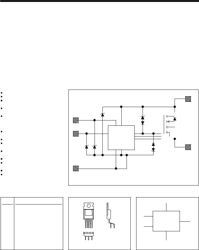
Fig.1. |
Elements of the TOPFET HSS. |
|||
with external ground resistor |
|
|
|
|
|
PINNING - SOT263 |
PIN CONFIGURATION |
SYMBOL |
|
||
PIN |
DESCRIPTION |
|
|
|
|
1 |
Ground |
tab |
|
|
|
|
|
|
|
||
2 |
Input |
|
|
I |
B |
|
|
TOPFET L |
|||
3 |
Battery (+ve supply) |
|
|
|
|
|
|
S |
HSS |
||
|
|
|
|
G |
|
4 |
Status |
1 2 3 4 5 |
|
|
|
leadform |
|
|
|||
5 |
Load |
263-01 |
|
|
|
Fig. 2. |
|
|
Fig. 3. |
||
tab |
connected to pin 3 |
|
|
||
|
|
|
|
||
April 1995 |
1 |
|
|
Rev 1.100 |
|

Philips Semiconductors Product specification
PowerMOS transistor |
|
|
|
|
BUK202-50X |
|
|||||
TOPFET high side switch |
|
|
|
|
|
|
|
|
|
|
|
|
|
|
|
|
|
|
|
|
|
|
|
LIMITING VALUES |
|
|
|
|
|
|
|
|
|
|
|
Limiting values in accordance with the Absolute Maximum System (IEC 134) |
|
|
|
|
|
|
|
|
|||
|
|
|
|
|
|
|
|
|
|||
SYMBOL |
PARAMETER |
|
CONDITIONS |
MIN. |
|
MAX. |
|
UNIT |
|
||
|
|
|
|
|
|
|
|
|
|
|
|
|
Battery voltages |
|
|
|
|
|
|
|
|
|
|
VBG |
Continuous off-state supply voltage |
- |
0 |
|
|
50 |
|
V |
|
||
|
Reverse battery voltages1 |
|
External resistors: |
|
|
|
|
|
|
|
|
-VBG |
Repetitive peak supply voltage |
|
RG ³150 W; RI = RS ³ 4.7 kW, |
- |
|
|
32 |
|
V |
|
|
|
|
|
d £ 0.1 |
|
|
|
|
|
|
|
|
-VBG |
Continuous reverse supply voltage |
RG ³150 W; RI = RS ³ 4.7 kW |
- |
|
|
16 |
|
V |
|
||
|
|
|
|
|
|
|
|
|
|
|
|
IL |
Continuous load current |
|
Tmb £ 110 ˚C |
- |
|
|
20 |
|
A |
|
|
PD |
Total power dissipation |
|
Tmb £ 25 ˚C |
- |
|
125 |
|
W |
|
||
Tstg |
Storage temperature |
|
- |
-55 |
|
175 |
|
˚C |
|
||
T |
Continuous junction temperature2 |
- |
- |
|
150 |
|
˚C |
|
|||
j |
|
|
|
|
|
|
|
|
|
|
|
Tsold |
Lead temperature |
|
during soldering |
- |
|
250 |
|
˚C |
|
||
|
Input and status |
|
|
|
|
|
|
|
|
|
|
II |
Continuous input current |
|
- |
-5 |
|
|
5 |
|
mA |
|
|
IS |
Continuous status current |
|
- |
-5 |
|
|
5 |
|
mA |
|
|
II |
Repetitive peak input current |
|
d £ 0.1 |
-20 |
|
|
20 |
|
mA |
|
|
IS |
Repetitive peak status current |
|
d £ 0.1 |
-20 |
|
|
20 |
|
mA |
|
|
|
|
|
|
|
|
|
|
|
|
|
|
|
Inductive load clamping |
|
|
|
|
|
|
|
|
|
|
EBL |
Non-repetitive clamping energy |
|
Tmb = 150 ˚C prior to turn-off |
- |
|
1.7 |
|
J |
|
||
ESD LIMITING VALUE |
|
|
|
|
|
|
|
|
|
|
|
|
|
|
|
|
|
|
|
|
|
||
SYMBOL |
PARAMETER |
|
CONDITIONS |
MIN. |
|
MAX. |
|
UNIT |
|
||
|
|
|
|
|
|
|
|
|
|
|
|
VC |
Electrostatic discharge capacitor |
|
Human body model; |
- |
|
|
2 |
|
kV |
|
|
|
voltage |
|
C = 250 pF; R = 1.5 kW |
|
|
|
|
|
|
|
|
THERMAL CHARACTERISTICS |
|
|
|
|
|
|
|
|
|
|
|
|
|
|
|
|
|
|
|
|
|
|
|
SYMBOL |
PARAMETER |
CONDITIONS |
MIN. |
TYP. |
|
MAX. |
UNIT |
|
|||
|
|
|
|
|
|
|
|
|
|
|
|
|
Thermal resistance3 |
|
|
|
|
|
|
|
|
|
|
Rth j-mb |
Junction to mounting base |
- |
|
- |
0.8 |
|
1 |
|
K/W |
|
|
Rth j-a |
Junction to ambient |
in free air |
- |
60 |
|
75 |
|
K/W |
|
||
1 Reverse battery voltage is allowed only with external ground, input and status resistors to limit the currents to a safe value.
2 For normal continuous operation. A higher Tj is allowed as an overload condition but at the threshold Tj(TO) the over temperature trip operates to protect the switch.
3 Of the output Power MOS transistor.
April 1995 |
2 |
Rev 1.100 |

Philips Semiconductors Product specification
PowerMOS transistor |
|
|
|
|
|
|
|
|
|
|
BUK202-50X |
|
|||
TOPFET high side switch |
|
|
|
|
|
|
|
|
|
|
|
|
|
|
|
|
|
|
|
|
|
|
|
|
|
|
|
|
|
|
|
STATIC CHARACTERISTICS |
|
|
|
|
|
|
|
|
|
|
|
|
|
|
|
Tmb = 25 ˚C unless otherwise stated |
|
|
|
|
|
|
|
|
|
|
|
|
|
|
|
|
|
|
|
|
|
|
|
|
|
|
|
||||
SYMBOL |
PARAMETER |
CONDITIONS |
|
|
|
|
MIN. |
TYP. |
MAX. |
UNIT |
|
||||
|
|
|
|
|
|
|
|
|
|
|
|
|
|
|
|
|
Clamping voltages |
|
|
|
|
|
|
|
|
|
|
|
|
|
|
VBG |
Battery to ground |
IG = 1 mA |
|
|
|
|
|
|
|
50 |
55 |
65 |
V |
|
|
VBL |
Battery to load |
IL = IG = 1 mA |
|
|
|
|
|
50 |
55 |
65 |
V |
|
|||
-VLG |
Negative load to ground |
IL = 1 mA |
|
|
|
|
|
|
|
12 |
17 |
21 |
V |
|
|
|
|
|
|
|
|
|
|
|
|
||||||
|
Supply voltage |
battery to ground |
|
|
|
|
|
|
|
||||||
V |
Operating range1 |
- |
|
|
|
|
|
|
|
|
5 |
- |
40 |
V |
|
BG |
|
|
|
|
|
|
|
|
|
|
|
|
|
|
|
|
Currents |
VBG = 13 V |
|
|
|
|
|
|
|
|
|
|
|
|
|
I |
Nominal load current2 |
V |
= 0.5 V; T |
mb |
= 85 ˚C |
|
9 |
- |
- |
A |
|
||||
L |
|
BL |
|
|
|
|
|
|
|
|
|
|
|
||
I |
Quiescent current3 |
V |
= 0 V; V |
LG |
= 0 V |
|
|
- |
0.1 |
2 |
μA |
|
|||
B |
|
IG |
|
|
|
|
|
|
|
|
|
|
|
||
I |
Operating current4 |
V |
= 5 V; I = 0 A |
|
|
1.5 |
2.2 |
4 |
mA |
|
|||||
G |
|
IG |
L |
|
|
|
|
|
|
|
|
|
|
|
|
I |
Off-state load current5 |
V |
= 13 V; V |
|
= 0 V |
|
|
- |
0.1 |
1 |
μA |
|
|||
L |
|
BL |
|
|
IG |
|
|
|
|
|
|
|
|
|
|
|
Resistances |
|
|
|
|
|
|
|
|
|
|
|
|
|
|
R |
On-state resistance6 |
V |
= 13 V; I |
L |
= 10 A; t |
p |
= 300 μs |
- |
28 |
38 |
mΩ |
|
|||
ON |
|
BG |
|
|
|
|
|
|
|
|
|
|
|
||
RON |
On-state resistance |
VBG = 5 V; IL = 2 A; tp = 300 μs |
- |
36 |
48 |
mΩ |
|
||||||||
INPUT CHARACTERISTICS |
|
|
|
|
|
|
|
|
|
|
|
|
|
|
|
Tmb = 25 ˚C; VBG = 13 V |
|
|
|
|
|
|
|
|
|
|
|
|
|
|
|
SYMBOL |
PARAMETER |
CONDITIONS |
|
|
|
|
MIN. |
TYP. |
MAX. |
UNIT |
|
||||
|
|
|
|
|
|
|
|
|
|
|
|
|
|
|
|
II |
Input current |
VIG = 5 V |
|
|
|
|
|
|
|
35 |
60 |
100 |
μA |
|
|
VIG |
Input clamping voltage |
II = 200 μA |
|
|
|
|
|
|
|
6 |
7 |
8 |
V |
|
|
VIG(ON) |
Input turn-on threshold voltage |
|
|
|
|
|
|
|
|
|
- |
2.1 |
2.4 |
V |
|
VIG(OFF) |
Input turn-off threshold voltage |
|
|
|
|
|
|
|
|
|
1.5 |
1.7 |
- |
V |
|
VIG |
Input turn-on hysteresis |
|
|
|
|
|
|
|
|
|
- |
0.4 |
- |
V |
|
1 On-state resistance is increased if the supply voltage is less than 9 V. Refer to figure 8.
2 Defined as in ISO 10483-1.
3 This is the continuous current drawn from the battery when the input is low and includes leakage current to the load.
4 This is the continuous current drawn from the battery with no load connected, but with the input high.
5 The measured current is in the load pin only.
6 The supply and input voltage for the RON tests are continuous. The specified pulse duration tp refers only to the applied load current.
April 1995 |
3 |
Rev 1.100 |
Philips Semiconductors Product specification
PowerMOS transistor |
|
|
|
|
|
|
BUK202-50X |
|
|||
TOPFET high side switch |
|
|
|
|
|
|
|
|
|
|
|
|
|
|
|
|
|
|
|||||
PROTECTION FUNCTIONS AND STATUS INDICATIONS |
|
|
|
|
|
|
|||||
Truth table for normal, open-circuit load and overload conditions and abnormal supply voltages. |
|
|
|
||||||||
|
|
|
|
|
|
|
|
||||
|
FUNCTIONS |
|
TRUTH TABLE |
|
THRESHOLD |
|
|
||||
SYMBOL |
CONDITION |
INPUT |
|
STATUS |
OUTPUT |
MIN. |
TYP. |
MAX. |
UNIT |
|
|
|
|
|
|
|
|
|
|
|
|
|
|
|
Normal on-state |
1 |
|
1 |
|
1 |
|
|
|
|
|
|
|
|
|
|
|
|
|
|
|
|
|
|
Normal off-state |
0 |
|
1 |
|
0 |
|
|
|
|
|
|
|
|
|
|
|
|
|
|
|
|
|
I |
Open circuit load1 |
1 |
|
0 |
|
1 |
150 |
450 |
750 |
mA |
|
L(OC) |
|
|
|
|
|
|
|
|
|
|
|
|
Open circuit load |
0 |
|
1 |
|
0 |
|
|
|
|
|
|
|
|
|
|
|
|
|
|
|
|
|
T |
Over temperature2 |
1 |
|
0 |
|
0 |
150 |
175 |
- |
˚C |
|
j(TO) |
|
|
|
|
|
|
|
|
|
|
|
|
Over temperature3 |
0 |
|
0 |
|
0 |
|
|
|
|
|
V |
Short circuit load4 |
1 |
|
0 |
|
0 |
9 |
10.5 |
12 |
V |
|
BL(TO) |
|
|
|
|
|
|
|
|
|
|
|
|
Short circuit load |
0 |
|
1 |
|
0 |
|
|
|
|
|
|
|
|
|
|
|
|
|
|
|
|
|
V |
Low supply voltage5 |
X |
|
1 |
|
0 |
3 |
4 |
5 |
V |
|
BG(TO) |
|
|
|
|
|
|
|
|
|
|
|
V |
High supply voltage6 |
X |
|
1 |
|
0 |
40 |
45 |
50 |
V |
|
BG(LP) |
|
|
|
|
|
|
|
|
|
|
|
For input `0' equals low, `1' equals high, `X' equals don't care.
For status `0' equals low, `1' equals open or high.
For output switch `0' equals off, `1' equals on.
STATUS CHARACTERISTICS
Tmb = 25 ˚C.
The status output is an open drain transistor, and requires an external pull-up circuit to indicate a logic high.
SYMBOL |
PARAMETER |
CONDITIONS |
|
|
MIN. |
TYP. |
MAX. |
UNIT |
||
|
|
|
|
|
|
|
|
|
|
|
VSG |
Status clamping voltage |
IS = 100 μA |
|
|
|
|
6 |
7 |
8 |
V |
VSG |
Status low voltage |
IS = 50 μA; VBG = 13 V |
|
|
- |
0.7 |
0.8 |
V |
||
IS |
Status leakage current |
VSG = 5 V |
|
|
|
|
- |
0.1 |
1 |
μA |
I |
Status saturation current13 |
V = 5 V; R |
S |
= 0 Ω; V |
BG |
= 13 V |
- |
9 |
- |
mA |
S |
|
SS |
|
|
|
|
|
|
||
|
Application information |
|
|
|
|
|
R |
External pull-up resistor8 |
V = 5 V |
- |
100 |
- |
kΩ |
S |
|
SS |
|
|
|
|
1 In the on-state, the switch detects whether the load current is less than the quoted open load threshold current. This is for status indication only. Typical hysteresis equals 230 mA. The thresholds are specified for supply voltage within the normal working range.
2 After cooling below the reset temperature the switch will resume normal operation. The reset temperature is lower than the trip temperature by typically 10 ˚C.
3 If the overtemperature protection has operated, status remains low to indicate the overtemperature condition even if the input is taken low, providing the device has not cooled below the reset temperature.
4 After short circuit protection has operated, the input voltage must be toggled low for the switch to resume normal operation.
5 Undervoltage sensor causes the device to switch off. Typical hysteresis equals 0.5 V.
6 Overvoltage sensor causes the device to switch off to protect the load. Typical hysteresis equals 1.1 V.
7 In a fault condition with the pull-up resistor short circuited while the status transistor is conducting.
8 The pull-up resistor also protects the status pin during reverse battery conditions.
April 1995 |
4 |
Rev 1.100 |

Philips Semiconductors Product specification
PowerMOS transistor |
|
|
|
|
|
BUK202-50X |
|
|||
TOPFET high side switch |
|
|
|
|
|
|
|
|
|
|
|
|
|
|
|
|
|
|
|
|
|
DYNAMIC CHARACTERISTICS |
|
|
|
|
|
|
|
|
|
|
Tmb = 25 ˚C; VBG = 13 V |
|
|
|
|
|
|
|
|
|
|
|
|
|
|
|
|
|
|
|
|
|
SYMBOL |
PARAMETER |
CONDITIONS |
|
|
MIN. |
TYP. |
MAX. |
UNIT |
|
|
|
|
|
|
|
|
|
|
|
|
|
|
Inductive load turn-off |
|
|
|
|
|
|
|
|
|
-V |
Negative load voltage1 |
V |
= 0 V; I = 10 A; t |
p |
= 300 μs |
15 |
20 |
25 |
V |
|
LG |
|
IG |
L |
|
|
|
|
|
|
|
|
Short circuit load protection2 |
V |
= 5 V; R ≤ 10 mΩ |
|
|
|
|
|
|
|
|
|
IG |
L |
|
|
|
|
|
|
|
td sc |
Response time |
VIG = 5 V |
|
|
- |
75 |
- |
μs |
|
|
IL |
Load current prior to turn-off |
t < td sc |
|
|
- |
50 |
- |
A |
|
|
|
Overload protection3 |
|
|
|
|
|
|
|
|
|
IL(lim) |
Load current limiting |
VBL = 9 V; tp = 300 μs |
|
34 |
45 |
64 |
A |
|
||
SWITCHING CHARACTERISTICS |
|
|
|
|
|
|
|
|
|
|
Tmb = 25 ˚C, VBG = 13 V, for resistive load RL = 13 Ω. |
|
|
|
|
|
|
|
|||
SYMBOL |
PARAMETER |
CONDITIONS |
|
|
MIN. |
TYP. |
MAX. |
UNIT |
|
|
|
|
|
|
|
|
|
|
|
|
|
|
During turn-on |
to VIG = 5 V |
|
|
|
|
|
|
|
|
td on |
Delay time |
to 10% VL |
|
|
- |
16 |
- |
μs |
|
|
dV/dton |
Rate of rise of load voltage |
|
|
|
|
- |
0.7 |
2 |
V/μs |
|
t on |
Total switching time |
to 90% VL |
|
|
- |
140 |
- |
μs |
|
|
td off
dV/dtoff
t off
During turn-off |
to VIG = 0 V |
|
|
|
|
Delay time |
to 90% VL |
- |
40 |
- |
μs |
Rate of fall of load voltage |
|
- |
0.7 |
2 |
V/μs |
Total switching time |
to 10% VL |
- |
70 |
- |
μs |
|
|
|
|
|
|
CAPACITANCES
Tmb = 25 ˚C; f = 1 MHz; VIG = 0 V
SYMBOL |
PARAMETER |
CONDITIONS |
MIN. |
TYP. |
MAX. |
UNIT |
|
|
|
|
|
|
|
Cig |
Input capacitance |
VBG = 13 V |
- |
15 |
20 |
pF |
Cbl |
Output capacitance |
VBL = VBG = 13 V |
- |
500 |
700 |
pF |
Csg |
Status capacitance |
VSG = 5 V |
- |
11 |
15 |
pF |
1 For a high side switch, the load pin voltage goes negative with respect to ground during the turn-off of an inductive load. This negative voltage is clamped by the device.
2 The load current is self-limited during the response time for short circuit load protection. Response time is measured from when input goes high.
3 If the load resistance is low, but not a complete short circuit, such that the on-state voltage remains less than VBL(TO), the device remains in current limiting until the overtemperature protection operates.
April 1995 |
5 |
Rev 1.100 |