Материал: WT7520
WT7520
Data Sheet Rev. 0.90
APPLICATION NOTE
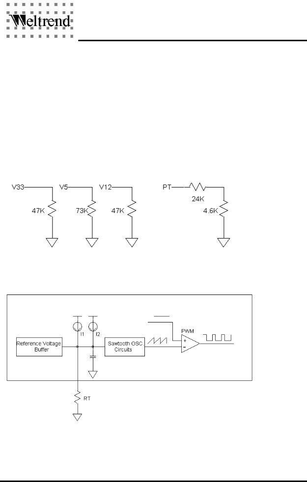
1.Input impedance:
Pin No. |
Pin Name |
Input impedance |
1 |
V33 |
47KΩ |
|
|
|
2 |
V5 |
73KΩ |
|
|
|
3 |
V12 |
47KΩ |
|
|
|
4 |
PT |
24 KΩ+4.6 KΩ |
|
|
|
2.Sawtooth OSC. Funcition:
Weltrend Semiconductor, Inc.
Page 6
WT7520
Data Sheet Rev. 0.90
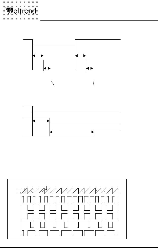
3.REMOTE ON/OFF
REM
REMONF |
|
|
|
|
trem |
|
|
|
trem |
|||||||
|
|
|
|
|
||||||||||||
REMON |
|
|
|
|
|
|
|
|
|
|
|
|
|
|
|
|
|
|
|
|
|
|
|
|
|
|
|
|
|
|
|
||
|
|
|
|
|
|
toff |
|
|
|
|
toff |
|||||
|
|
|
|
|
|
|
|
|
||||||||
SS |
|
|
|
|
|
|
|
|
|
|
|
|
|
|
|
|
|
|
|
|
|
|
|
|
|
|
|
|
|
|
|
|
|
|
|
|
|
|
|
|
|
|
|
|
|
|
|
|
|
|
|
|
|
|
|
|
|
|
|
|
|
|
|
|
|
|
|
4. Under Voltage Protection Delay Time
REM
REMON
td,uvp
UVP
5. Pulse Width Modulation Block
The output pulse width modulation is generated by comparision of the saw–tooth waveform from the capacitor CT to the feedback of the voltage.
Therefore, an increase in feedback control signal amplitude cause a linear decrease of the output pulse width. Also, the SS(DTC and Soft-Start) limits the output pulse width. The timing diagram is shown as below:
PWM OUT
CT
DTC
FF-CLK
FF-Q
FF-QN
C1
C2
Weltrend Semiconductor, Inc.
Page 7
WT7520
Data Sheet Rev. 0.90
6. The function of “PT”:
This signal is prepared for extra OVP/OPP (VPT > 1.25V) or another Disable Under Voltage Protection function (VPT < 0.62V)
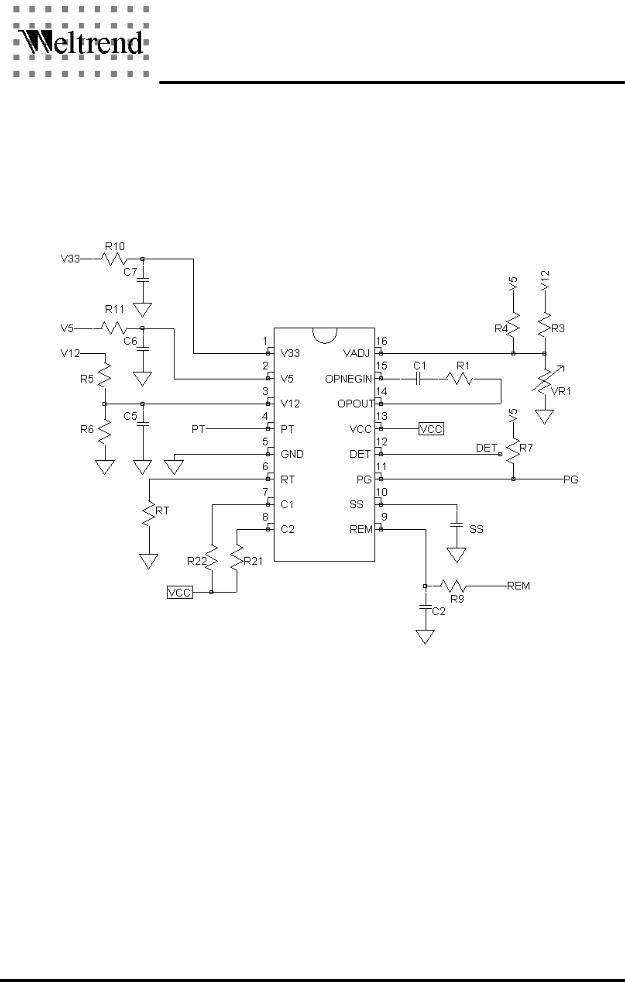
7. Reference Application Ciruit:
8. In some application power system, adding an external resistor (R9) could reduce the peak value spike from the environments to pin 9 (REM) and avoid pin 9 (REM ) damaged by the external noise.
Weltrend Semiconductor, Inc.
Page 8
WT7520
Data Sheet Rev. 0.90
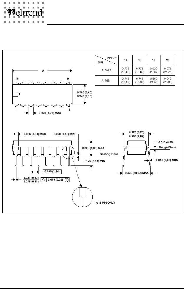
MECHANICAL INFORMATION
PLASTIC DUAL–IN–LINE PACKAGE
NOTE 1 All linear dimensions are in inches millimeters .
NOTE 2 This drawing is subject to change without notice.
NOTE 3 Falls within JEDEC MS–001
Weltrend Semiconductor, Inc.
Page 9