Материал: 9877
DISCRETE SEMICONDUCTORS
handbook, 2 columns
M3D116
BYW54 to BYW56
Controlled avalanche rectifiers
Product specification |
1996 Jun 11 |
Supersedes data of April 1992
File under Discrete Semiconductors, SC01
Philips Semiconductors |
Product specification |
|
|
|
|
Controlled avalanche rectifiers |
BYW54 to BYW56 |
|
|
|
|
FEATURES
∙Glass passivated
∙High maximum operating temperature
∙Low leakage current
∙Excellent stability
∙Guaranteed avalanche energy absorption capability
∙Available in ammo-pack.
LIMITING VALUES
DESCRIPTION |
This package is hermetically sealed |
|
Rugged glass package, using a high |
and fatigue free as coefficients of |
|
expansion of all used parts are |
||
temperature alloyed construction. |
||
matched. |
||
|
||
k |
a |
|
|
MAM047 |
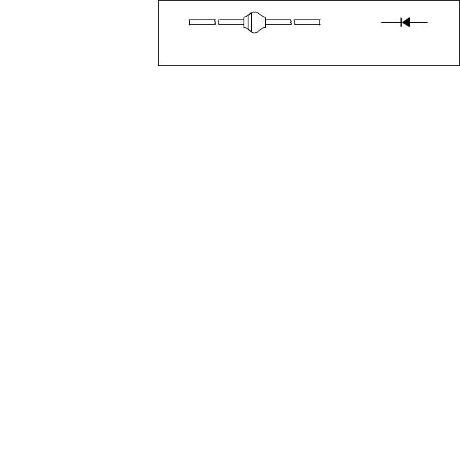
Fig.1 Simplified outline (SOD57) and symbol.
In accordance with the Absolute Maximum Rating System (IEC 134).
SYMBOL |
PARAMETER |
CONDITIONS |
MIN. |
MAX. |
UNIT |
|
|
|
|
|
|
|
|
VRRM |
repetitive peak reverse voltage |
|
|
|
|
|
|
BYW54 |
|
− |
600 |
V |
|
|
BYW55 |
|
− |
800 |
V |
|
|
BYW56 |
|
− |
1000 |
V |
|
|
|
|
|
|
|
|
VRWM |
crest working reverse voltage |
|
|
|
|
|
|
BYW54 |
|
− |
600 |
V |
|
|
BYW55 |
|
− |
800 |
V |
|
|
BYW56 |
|
− |
1000 |
V |
|
|
|
|
|
|
|
|
VR |
continuous reverse voltage |
|
|
|
|
|
|
BYW54 |
|
− |
600 |
V |
|
|
BYW55 |
|
− |
800 |
V |
|
|
BYW56 |
|
− |
1000 |
V |
|
|
|
|
|
|
|
|
IF(AV) |
average forward current |
Ttp = 45 °C; |
− |
2.0 |
A |
|
|
|
|
lead length = 10 mm; |
|
|
|
|
|
|
averaged over any 20 ms |
|
|
|
|
|
|
period; see Figs 2 and 4 |
|
|
|
|
|
|
|
|
|
|
|
|
|
Tamb = 80 °C; PCB mounting |
− |
0.8 |
A |
|
|
|
(see Fig.9); |
|
|
|
|
|
|
averaged over any 20 ms |
|
|
|
|
|
|
period; see Figs 3 and 4 |
|
|
|
|
|
|
|
|
|
|
IFSM |
non-repetitive peak forward current |
t = 10 ms half sinewave |
− |
50 |
A |
|
ERSM |
non-repetitive peak reverse avalanche |
L = 120 mH; Tj = Tj max prior to |
− |
20 |
mJ |
|
|
energy |
surge; inductive load switched off |
|
|
|
|
|
|
|
|
|
|
|
Tstg |
storage temperature |
|
−65 |
+175 |
°C |
|
Tj |
junction temperature |
see Fig.5 |
−65 |
+175 |
°C |
|
1996 Jun 11 |
2 |

Philips Semiconductors |
|
|
|
Product specification |
||||
|
|
|
|
|
|
|
|
|
Controlled avalanche rectifiers |
|
BYW54 to BYW56 |
||||||
|
|
|
|
|
|
|
|
|
ELECTRICAL CHARACTERISTICS |
|
|
|
|
|
|
||
Tj = 25 °C; unless otherwise specified. |
|
|
|
|
|
|
||
|
|
|
|
|
|
|
|
|
SYMBOL |
PARAMETER |
CONDITIONS |
MIN. |
TYP. |
|
MAX. |
UNIT |
|
|
|
|
|
|
|
|
|
|
VF |
forward voltage |
IF = 1 A; Tj = Tj max; see Fig.6 |
- |
- |
|
0.8 |
V |
|
|
|
|
IF = 1 A; see Fig.6 |
- |
- |
|
1.0 |
V |
V(BR)R |
reverse avalanche |
IR = 0.1 mA |
|
|
|
|
|
|
|
breakdown voltage |
|
|
|
|
|
|
|
|
BYW54 |
|
650 |
- |
|
- |
V |
|
|
BYW55 |
|
900 |
- |
|
- |
V |
|
|
BYW56 |
|
1100 |
- |
|
- |
V |
|
IR |
reverse current |
VR = VRRMmax; see Fig.7 |
- |
- |
|
1 |
mA |
|
|
|
|
VR = VRRMmax; Tj = 165 °C; |
- |
- |
|
150 |
mA |
|
|
|
see Fig.7 |
|
|
|
|
|
|
|
|
|
|
|
|
|
|
trr |
reverse recovery time |
when switched from IF = 0.5 A to |
- |
3 |
|
- |
ms |
|
|
|
|
IR = 1 A; measured at IR = 0.25 A; |
|
|
|
|
|
|
|
|
see Fig.10 |
|
|
|
|
|
|
|
|
|
|
|
|
|
|
Cd |
diode capacitance |
VR = 0 V; f = 1 MHz; see Fig.8 |
- |
50 |
|
- |
pF |
|
THERMAL CHARACTERISTICS
SYMBOL |
PARAMETER |
CONDITIONS |
VALUE |
UNIT |
|
|
|
|
|
Rth j-tp |
thermal resistance from junction to tie-point |
lead length = 10 mm |
46 |
K/W |
Rth j-a |
thermal resistance from junction to ambient |
note 1 |
100 |
K/W |
Note
1.Device mounted on epoxy-glass printed-circuit board, 1.5 mm thick; thickness of copper ³40 mm, see Fig.9. For more information please refer to the “General Part of Handbook SC01”.
1996 Jun 11 |
3 |
Philips Semiconductors |
Product specification |
|
|
Controlled avalanche rectifiers |
BYW54 to BYW56 |
|
|
GRAPHICAL DATA
MBG044
3 handbook, halfpage
IF(AV)
(A)
2
1
0 |
|
|
|
|
|
0 |
40 |
80 |
120 |
160 |
200 |
Ttp (°C)
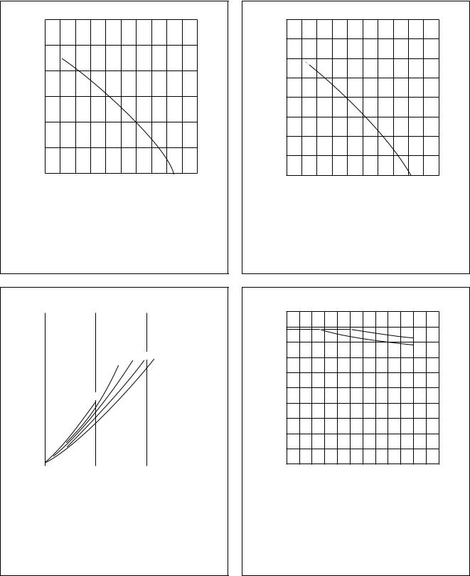
Switched mode application.
a = 1.57; VR = VRRMmax; δ = 0.5; lead length 10 mm.
Fig.2 Maximum permissible average forward current as a function of tie-point temperature (including losses due to reverse leakage).
MBG054
1.6 handbook, halfpage
IF(AV)
(A)
1.2
0.8
0.4
0
0 |
40 |
80 |
120 |
160 |
200 |
|
|
|
|
Tamb (°C) |
|
Switched mode application.
a = 1.57; VR = VRRMmax; δ = 0.5; device mounted as shown in Fig.9.
Fig.3 Maximum permissible average forward current as a function of ambient temperature (including losses due to reverse leakage).
MGC745
4 |
|
|
|
|
|
|
|
|
|
handbook, halfpage |
|
|
|
|
|
|
|
||
P |
|
|
|
|
|
|
|
|
|
(W) |
|
|
|
|
|
|
|
|
|
3 |
|
|
|
|
|
|
|
|
|
|
|
|
2.5 |
2 |
1.57 1.42 |
|
|
|
|
|
|
|
|
|
|
|
|||
|
|
|
|
|
|
|
|
|
|
2 |
|
|
|
|
|
|
|
|
|
|
|
|
|
|
|
|
|
|
|
|
|
a = 3 |
|
|
|
|
|
||
|
|
|
|
|
|
|
|
||
1 |
|
|
|
|
|
|
|
|
|
|
|
|
|
|
|
|
|
|
|
|
|
|
|
|
|
|
|
|
|
0 |
|
|
|
|
|
|
|
|
|
|
|
|
|
|
|
|
|
|
|
|
|
|
|
|
|
|
|
|
|
0 |
1 |
|
2 |
|
3 |
||||
|
|
|
|
|
|
IF(AV) (A) |
|
|
|
a = IF(RMS)/IF(AV); VR = VRRMmax; δ = 0.5. |
|
|
|
|
|||||
Fig.4 |
Maximum steady state power dissipation |
||||||||
|
|
(forward plus leakage current losses, |
|
|
|||||
|
|
excluding switching losses) as a function |
|||||||
|
|
of average forward current. |
|
|
|||||
MBH387
200
Tj (°C)
100
54 55 56
0
0 |
400 |
800 |
VR (V) |
1200 |
|
|
|
|
Solid line = VR.
Dotted line = VRRM; δ = 0.5.
Fig.5 Maximum permissible junction temperature as a function of reverse voltage.
1996 Jun 11 |
4 |
Philips Semiconductors |
Product specification |
|
|
Controlled avalanche rectifiers |
BYW54 to BYW56 |
|
|
MGC735
15 handbook, halfpage
IF
(A)
10
5
0
0 |
1 |
2 |
VF (V)
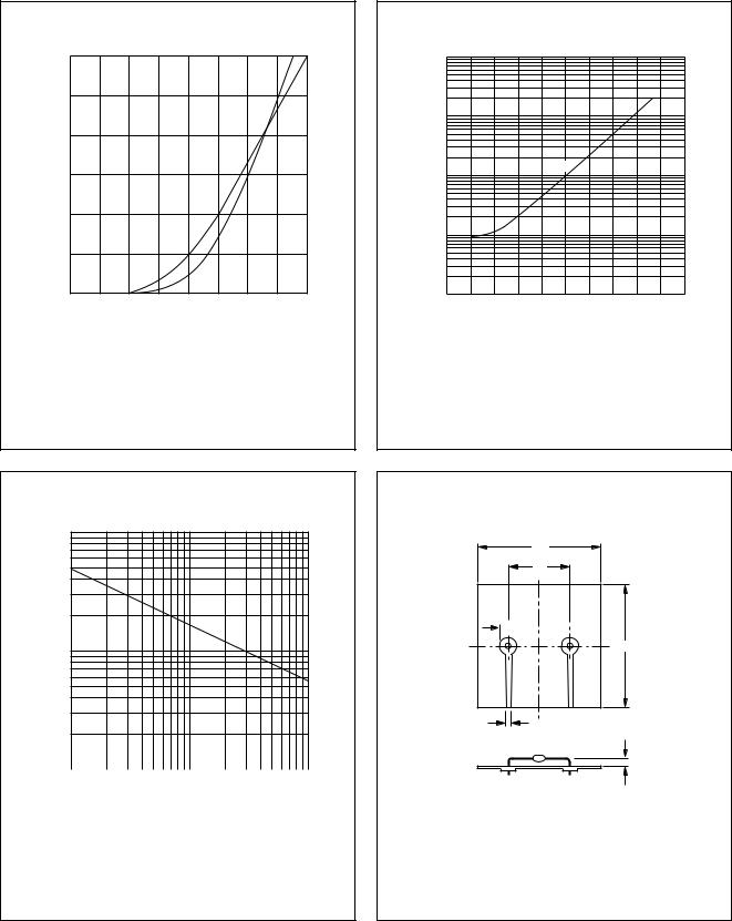
Solid line: Tj = 25 °C.
Dotted line: Tj = Tj max.
Fig.6 Forward current as a function of forward voltage; maximum values.
MGC734
103 handbook, halfpage
IR
(μA)
102
max
10
1
10 −1
0 |
40 |
80 |
120 |
160 |
200 |
o
Tj ( C)
VR = VRRMmax.
Fig.7 Reverse current as a function of junction temperature; maximum values.
MBG031
10 2 handbook, halfpage
Cd (pF)
10
1 |
|
|
|
|
|
|
|
|
|
|
102 |
||
1 |
10 |
VR |
(V) |
|||
|
|
|
|
|
||
f = 1 MHz; Tj = 25 °C.
Fig.8 Diode capacitance as a function of reverse voltage; typical values.
50
handbook, halfpage
25
7 

50
2
3
MGA200
Dimensions in mm.
Fig.9 Device mounted on a printed-circuit board.
1996 Jun 11 |
5 |