Материал: 2716
M2716
Table 8. Programming Mode AC Characteristics (1)
(TA = 25 °C; VCC = 5V ± 5%; VPP = 25V ± 1V)
Symbol |
Alt |
Parameter |
Test Condition |
Min |
Max |
Units |
tAVPH |
tAS |
Address Valid to Program High |
G = VIH |
2 |
|
μs |
tQVPH |
tDS |
Input Valid to Program High |
G = VIH |
2 |
|
μs |
tGHPH |
tOS |
Output Enable High to Program |
|
2 |
|
μs |
|
|
High |
|
|
||
|
|
|
|
|
|
|
tPL1PL2 |
tPR |
Program Pulse Rise Time |
|
5 |
|
ns |
tPH1PH2 |
tPF |
Program Pulse Fall Time |
|
5 |
|
ns |
tPHPL |
tPW |
Program Pulse Width |
|
45 |
55 |
ms |
tPLQX |
tDH |
Program Low to Input Transition |
|
2 |
|
μs |
tPLGX |
tOH |
Program Low to Output Enable |
|
2 |
|
μs |
|
|
Transition |
|
|
||
|
|
|
|
|
|
|
tGLQV |
tOE |
Output Enable to Output Valid |
EP = VIL |
|
120 |
ns |
tGHQZ |
tDF |
Output Enable High to Output Hi-Z |
|
0 |
100 |
ns |
tPLAX |
tAH |
Program Low to Address Transition |
|
2 |
|
μs |
Notes: 1. VCC must be applied simultaneously with or before VPP and removed simultaneously or after VPP. 2. Sampled only, not 100% tested.
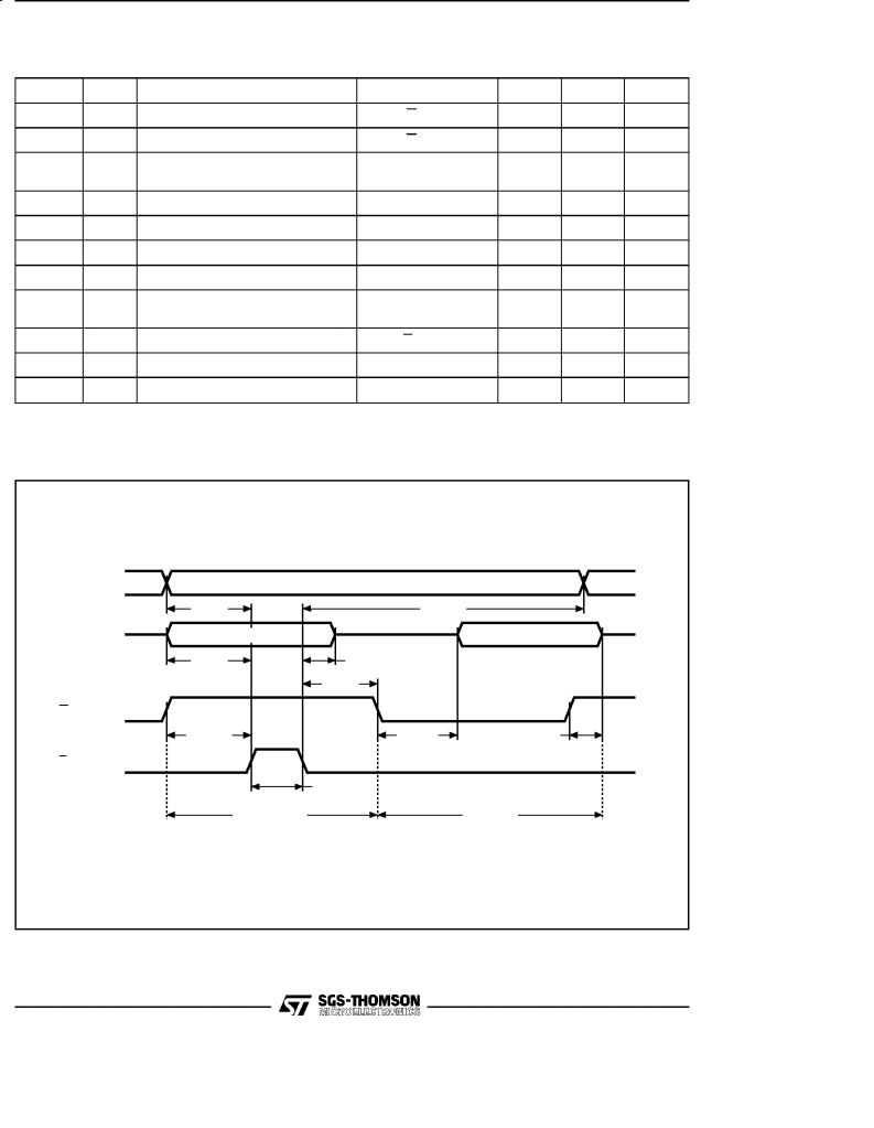
Figure 6. Programming and Verify Modes AC Waveforms
A0-A10 |
|
VALID |
|
|
tAVPH |
tPLAX |
|
Q0-Q7 |
DATA IN |
|
DATA OUT |
|
tQVPH |
tPLQX |
|
|
|
tPLGX |
|
G |
|
|
|
|
tGHPH |
tGLQV |
tGHQZ |
EP |
|
|
|
|
|
tPHPL |
|
|
PROGRAM |
|
VERIFY |
AI00787
6/9
M2716
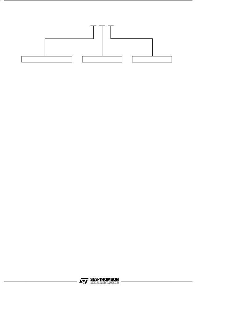
ORDERING INFORMATION SCHEME
Example: |
M2716 |
-1 F 1 |
Speed and VCC Tolerance |
|
Package |
Temperature Range |
||
-1 |
350 ns, 5V ±10% |
F |
FDIP24W |
1 |
0 to 70 °C |
blank |
450 ns, 5V ±5% |
|
|
6 |
±40 to 85 °C |
For a list of available options (Speed, VCC Tolerance, Package, etc...) refer to the current Memory Shortform catalogue.
For further information on any aspect of this device, please contact SGS-THOMSON Sales Office nearest to you.
7/9
M2716
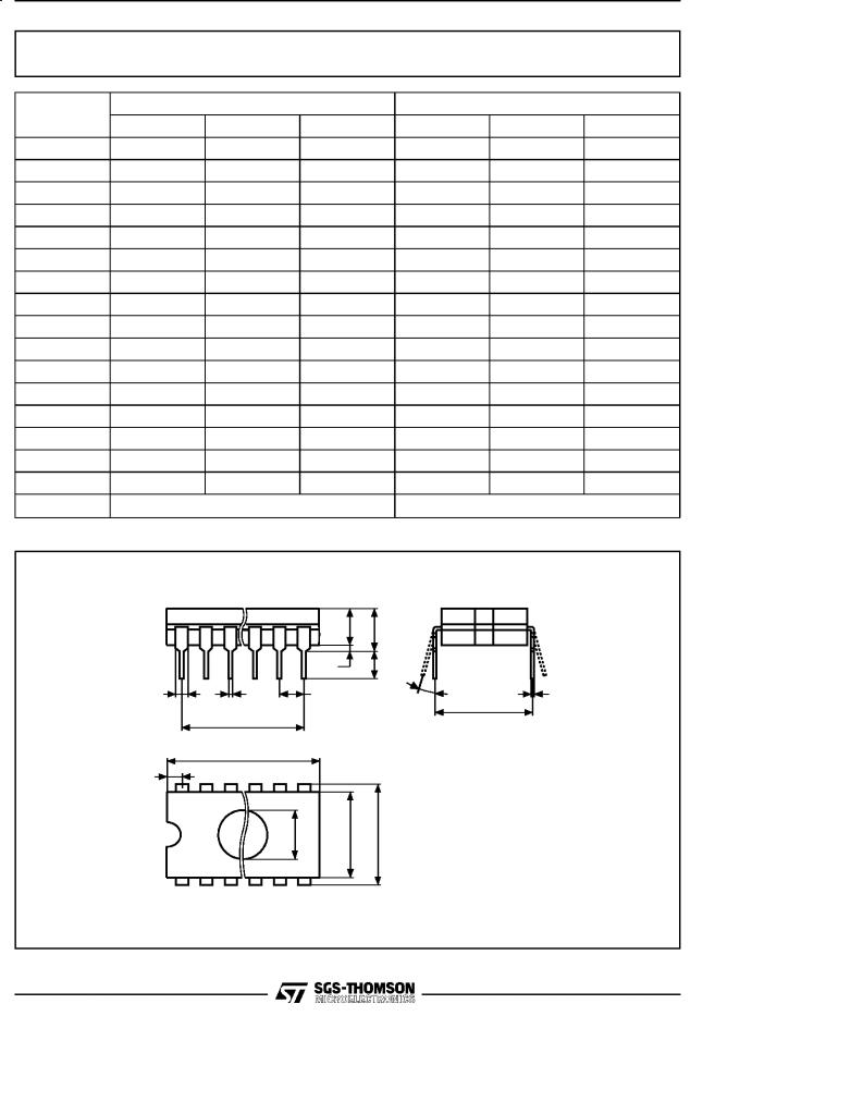
FDIP24W - 24 pin Ceramic Frit-seal DIP, with window
Symb |
|
mm |
|
|
inches |
|
|
Typ |
Min |
Max |
Typ |
Min |
Max |
||
|
|||||||
A |
|
|
5.71 |
|
|
0.225 |
|
A1 |
|
0.50 |
1.78 |
|
0.020 |
0.070 |
|
A2 |
|
3.90 |
5.08 |
|
0.154 |
0.200 |
|
B |
|
0.40 |
0.55 |
|
0.016 |
0.022 |
|
B1 |
|
1.17 |
1.42 |
|
0.046 |
0.056 |
|
C |
|
0.22 |
0.31 |
|
0.009 |
0.012 |
|
D |
|
|
32.30 |
|
|
1.272 |
|
E |
|
15.40 |
15.80 |
|
0.606 |
0.622 |
|
E1 |
|
13.05 |
13.36 |
|
0.514 |
0.526 |
|
e1 |
2.54 |
± |
± |
0.100 |
± |
± |
|
e3 |
27.94 |
± |
± |
1.100 |
± |
± |
|
eA |
|
16.17 |
18.32 |
|
0.637 |
0.721 |
|
L |
|
3.18 |
4.10 |
|
0.125 |
0.161 |
|
S |
|
1.52 |
2.49 |
|
0.060 |
0.098 |
|
|
7.11 |
± |
± |
0.280 |
± |
± |
|
α |
|
4° |
15° |
|
4° |
15° |
|
N |
|
24 |
|
|
24 |
|
FDIP24W
|
|
A2 |
A |
|
|
|
A1 |
L |
|
B1 |
B |
e1 |
α |
C |
|
e3 |
|
|
eA |
|
|
|
|
|
|
D |
|
|
|
|
S |
|
|
|
|
N |
|
|
|
|
|
E1 |
E |
|
|
1 |
|
|
|
FDIPW-a
Drawing is not to scale
8/9

M2716
Information furnished is believed to be accurate and reliable. However, SGS-THOMSON Microelectronics assumes no responsibility for the consequences of use of such information nor for any infringement of patents or other rights of third parties which may result from its use. No license is granted by implication or otherwise under any patent or patent rights of SGS-THOMSON Microelectronics. Specifications mentioned in this publication are subject to change without notice. This publication supersedes and replaces all information previously supplied. SGS-THOMSON Microelectronics products are not authorized for use as critical components in life support devices or systems without express written approval of SGS-THOMSON Microelectronics.
1994 SGS-THOMSON Microelectronics - All Rights Reserved
SGS-THOMSON Microelectronics GROUP OF COMPANIES
Australia - Brazil - China - France - Germany - Hong Kong - Italy - Japan - Korea - Malaysia - Malta - Morocco - The Netherlands -
Singapore - Spain - Sweden - Switzerland - Taiwan - Thailand - United Kingdom - U.S.A.
9/9