Материал: mmdf2c03hdrev5
MOTOROLA
SEMICONDUCTOR TECHNICAL DATA
Order this document by MMDF2C03HD/D
Designer's Data Sheet
Medium Power Surface Mount Products
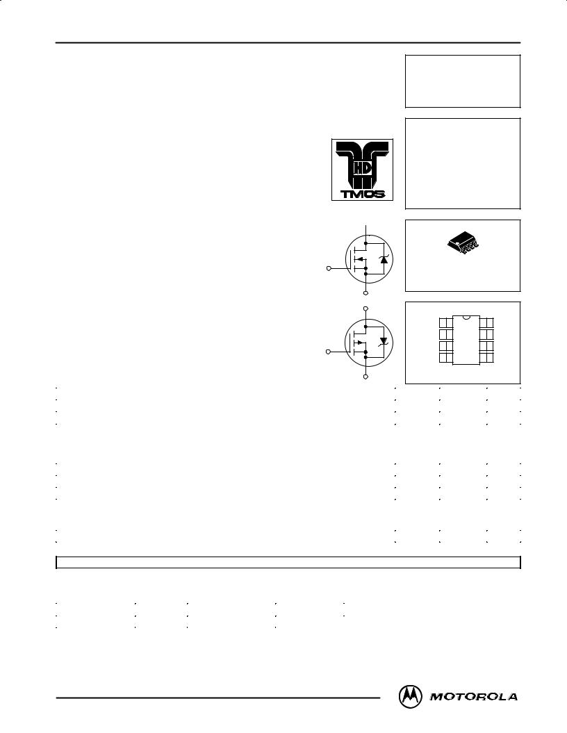
Complementary TMOS Field Effect Transistors
MiniMOS devices are an advanced series of power MOSFETs which utilize Motorola's High Cell Density HDTMOS process.
These miniature surface mount MOSFETs feature ultra low RDS(on) and true logic level performance. They are capable of withstanding
high energy in the avalanche and commutation modes and the drain-to-source diode has a very low reverse recovery time. MiniMOS devices are designed for use in low voltage, high speed switching applications where power efficiency is important. Typical applications are dc-dc converters, and power management in portable and battery powered products such as computers, printers, cellular and cordless phones. They can also be used for low voltage motor controls in mass storage products such as disk drives and tape drives. The avalanche energy is specified to eliminate the guesswork in designs where inductive loads are switched and offer additional safety margin against unexpected voltage transients.
•Ultra Low RDS(on) Provides Higher Efficiency and Extends Battery Life
•Logic Level Gate Drive Ð Can Be Driven by Logic ICs
•Miniature SO-8 Surface Mount Package Ð Saves Board Space
•Diode Is Characterized for Use In Bridge Circuits
•Diode Exhibits High Speed, With Soft Recovery
•IDSS Specified at Elevated Temperature
•Avalanche Energy Specified
•Mounting Information for SO-8 Package Provided
MAXIMUM RATINGS (TJ = 25°C unless otherwise noted)(1)
|
MMDF2C03HD |
|
|
Motorola Preferred Device |
|
|
COMPLEMENTARY |
|
|
DUAL TMOS POWER FET |
|
|
2.0 AMPERES |
|
|
30 VOLTS |
|
|
RDS(on) = 0.070 OHM |
|
|
(N-CHANNEL) |
|
RDS(on) = 0.200 OHM |
||
|
||
|
(P-CHANNEL) |
D 
N±Channel
G |
CASE 751±05, Style 14 |
||||
|
|
SO±8 |
|
|
|
|
S |
|
|
|
|
P±Channel |
D |
|
|
|
|
N±Source |
1 |
8 |
N±Drain |
||
|
|||||
|
N±Gate |
2 |
7 |
N±Drain |
|
G |
P±Source |
3 |
6 |
P±Drain |
|
P±Gate |
4 |
5 |
P±Drain |
||
|
|||||
|
S |
Top View |
|
||
|
|
|
|
||
|
Rating |
|
Symbol |
Value |
Unit |
|
|
|
|
|
|
Drain±to±Source Voltage |
|
|
VDSS |
30 |
Vdc |
Gate±to±Source Voltage |
|
|
VGS |
± 20 |
Vdc |
Drain Current Ð Continuous |
N±Channel |
|
ID |
4.1 |
A |
|
P±Channel |
|
|
3.0 |
|
Drain Current Ð Pulsed |
N±Channel |
|
IDM |
21 |
|
|
P±Channel |
|
|
15 |
|
Operating and Storage Temperature Range |
|
TJ, Tstg |
± 55 to 150 |
°C |
|
Total Power Dissipation @ T = 25°C (2) |
|
P |
2.0 |
Watts |
|
|
A |
|
D |
|
|
Thermal Resistance Ð Junction to Ambient (2) |
|
RqJA |
62.5 |
°C/W |
|
Single Pulse Drain±to±Source Avalanche Energy Ð Starting T J = 25°C |
|
EAS |
|
mJ |
|
(VDD = 30 V, VGS = 5.0 V, Peak IL = 9.0 Apk, L = 8.0 mH, RG = 25 W) |
N±Channel |
|
324 |
|
|
(VDD = 30 V, VGS = 5.0 V, Peak IL = 6.0 Apk, L = 18 mH, RG = 25 W) |
P±Channel |
|
324 |
|
|
Maximum Lead Temperature for Soldering, 0.0625″ from case. Time in Solder Bath is 10 seconds. |
TL |
260 |
°C |
||
DEVICE MARKING
D2C03
(1)Negative signs for P±Channel device omitted for clarity.
(2)Mounted on 2º square FR4 board (1º sq. 2 oz. Cu 0.06º thick single sided) with one die operating, 10 sec. max.
ORDERING INFORMATION
Device |
Reel Size |
Tape Width |
Quantity |
|
|
|
|
MMDF2C03HDR2 |
13″ |
12 mm embossed tape |
2500 units |
Designer's Data for ªWorst Caseº Conditions Ð The Designer' s Data Sheet permits the design of most circuits entirely from the information presented. SOA Limit curves Ð representing boundaries on device characteristics Ð are given to facilitate ªworst caseº design.
HDTMOS and MiniMOS are trademarks of Motorola, Inc. TMOS is a registered trademark of Motorola, Inc. Thermal Clad is a trademark of the Bergquist Company.
Preferred devices are Motorola recommended choices for future use and best overall value.
REV 5
Motorola, Inc. 1996

MMDF2C03HD |
|
|
|
|
|
|
|
|
|
ELECTRICAL CHARACTERISTICS (T = 25°C unless otherwise noted)(1) |
|
|
|
|
|
|
|||
|
|
A |
|
|
|
|
|
|
|
Characteristic |
Symbol |
Polarity |
Min |
Typ |
Max |
|
Unit |
||
|
|
|
|
|
|
|
|
|
|
OFF CHARACTERISTICS |
|
|
|
|
|
|
|
|
|
|
|
|
|
|
|
|
|
|
|
Drain±Source Breakdown Voltage |
|
V(BR)DSS |
|
|
|
|
|
Vdc |
|
(VGS = 0 Vdc, ID = 250 μAdc) |
|
|
Ð |
30 |
Ð |
Ð |
|
|
|
Zero Gate Voltage Drain Current |
|
IDSS |
(N) |
Ð |
Ð |
1.0 |
|
μAdc |
|
(VDS = 30 Vdc, VGS = 0 Vdc) |
|
|
(P) |
Ð |
Ð |
1.0 |
|
|
|
Gate±Body Leakage Current (VGS = ± 20 Vdc, VDS = 0) |
IGSS |
Ð |
Ð |
Ð |
100 |
|
nAdc |
||
ON CHARACTERISTICS(2) |
|
|
|
|
|
|
|
|
|
Gate Threshold Voltage |
|
VGS(th) |
(N) |
1.0 |
1.7 |
3.0 |
|
Vdc |
|
(VDS = VGS, ID = 250 μAdc) |
|
|
(P) |
1.0 |
1.5 |
2.0 |
|
|
|
Drain±to±Source On±Resistance |
|
RDS(on) |
(N) |
Ð |
0.06 |
0.070 |
|
Ohm |
|
(VGS = 10 Vdc, ID = 3.0 Adc) |
|
|
|
|
|||||
(VGS = 10 Vdc, ID = 2.0 Adc) |
|
|
(P) |
Ð |
0.17 |
0.200 |
|
|
|
Drain±to±Source On±Resistance |
|
RDS(on) |
(N) |
Ð |
0.065 |
0.075 |
|
Ohm |
|
(VGS = 4.5 Vdc, ID = 1.5 Adc) |
|
|
|
|
|||||
(VGS = 4.5 Vdc, ID = 1.0 Adc) |
|
|
(P) |
Ð |
0.225 |
0.300 |
|
|
|
Forward Transconductance |
|
gFS |
(N) |
2.0 |
3.6 |
Ð |
|
mhos |
|
(VDS = 3.0 Vdc, ID = 1.5 Adc) |
|
|
|
|
|||||
(VDS = 3.0 Vdc, ID = 1.0 Adc) |
|
|
(P) |
2.0 |
3.4 |
Ð |
|
|
|
DYNAMIC CHARACTERISTICS |
|
|
|
|
|
|
|
|
|
|
|
|
|
|
|
|
|
|
|
Input Capacitance |
|
|
Ciss |
(N) |
Ð |
450 |
630 |
|
pF |
|
|
|
|
(P) |
Ð |
397 |
550 |
|
|
|
|
(VDS = 24 Vdc, VGS = 0 |
|
|
|
|
|
|
|
Output Capacitance |
|
Coss |
(N) |
Ð |
160 |
225 |
|
|
|
|
Vdc, |
|
|
||||||
|
|
|
(P) |
Ð |
189 |
250 |
|
|
|
|
|
f = 1.0 MHz) |
|
|
|
||||
|
|
|
|
|
|
|
|
|
|
Transfer Capacitance |
|
|
Crss |
(N) |
Ð |
35 |
70 |
|
|
|
|
|
|
(P) |
Ð |
64 |
126 |
|
|
|
|
|
|
|
|
|
|
|
|
SWITCHING CHARACTERISTICS(3) |
|
|
|
|
|
|
|
|
|
Turn±On Delay Time |
|
(VDD = 15 Vdc, ID = 3.0 |
td(on) |
(N) |
Ð |
12 |
24 |
|
ns |
|
|
Adc, |
|
(P) |
Ð |
16 |
32 |
|
|
|
|
|
|
|
|
|
|
|
|
Rise Time |
|
VGS = 4.5 Vdc, |
t |
(N) |
Ð |
65 |
130 |
|
|
|
|
RG = 9.1 Ω) |
r |
(P) |
Ð |
18 |
36 |
|
|
|
|
|
|
|
|||||
Turn±Off Delay Time |
|
(VDD = 15 Vdc, ID = 2.0 |
td(off) |
(N) |
Ð |
16 |
32 |
|
|
|
|
Adc, |
|
(P) |
Ð |
63 |
126 |
|
|
|
|
|
|
|
|
|
|
|
|
Fall Time |
|
VGS = 4.5 Vdc, |
t |
(N) |
Ð |
19 |
38 |
|
|
|
|
RG = 6.0 Ω) |
f |
(P) |
Ð |
194 |
390 |
|
|
|
|
|
|
|
|||||
Turn±On Delay Time |
|
(VDD = 15 Vdc, ID = 3.0 |
td(on) |
(N) |
Ð |
8.0 |
16 |
|
|
|
|
Adc, |
|
(P) |
Ð |
9.0 |
18 |
|
|
|
|
|
|
|
|
|
|
|
|
Rise Time |
|
VGS = 10 Vdc, |
t |
(N) |
Ð |
15 |
30 |
|
|
|
|
RG = 9.1 Ω) |
r |
(P) |
Ð |
10 |
20 |
|
|
|
|
|
|
|
|||||
Turn±Off Delay Time |
|
(VDD = 15 Vdc, ID = 2.0 |
td(off) |
(N) |
Ð |
30 |
60 |
|
|
|
|
Adc, |
|
(P) |
Ð |
81 |
162 |
|
|
|
|
|
|
|
|
|
|
|
|
|
|
VGS = 10 Vdc, |
|
|
|
|
|
|
|
Fall Time |
|
tf |
(N) |
Ð |
23 |
46 |
|
|
|
|
|
RG = 6.0 Ω) |
|
(P) |
Ð |
192 |
384 |
|
|
Total Gate Charge |
|
|
QT |
(N) |
Ð |
11.5 |
16 |
|
nC |
|
|
|
|
(P) |
Ð |
14.2 |
19 |
|
|
|
|
(VDS = 10 Vdc, ID = 3.0 Adc, |
|
|
|
|
|
|
|
Gate±Source Charge |
|
Q1 |
(N) |
Ð |
1.5 |
Ð |
|
|
|
|
|
VGS = 10 Vdc) |
|
(P) |
Ð |
1.1 |
Ð |
|
|
Gate±Drain Charge |
|
(VDS = 24 Vdc, ID = 2.0 Adc, |
Q2 |
(N) |
Ð |
3.5 |
Ð |
|
|
|
|
VGS = 10 Vdc) |
|
(P) |
Ð |
4.5 |
Ð |
|
|
|
|
|
|
|
|
|
|
|
|
|
|
|
Q3 |
(N) |
Ð |
2.8 |
Ð |
|
|
|
|
|
|
(P) |
Ð |
3.5 |
Ð |
|
|
|
|
|
|
|
|
|
|
|
|
(1) Negative signs for P±Channel device omitted for clarity. |
|
|
|
|
|
(continued) |
|||
(2)Pulse Test: Pulse Width ≤ 300 μs, Duty Cycle ≤ 2%.
(3)Switching characteristics are independent of operating junction temperature.
2 |
Motorola TMOS Power MOSFET Transistor Device Data |
MMDF2C03HD
ELECTRICAL CHARACTERISTICS Ð continued (T = 25°C unless otherwise noted)(1) |
|
|
|
|
||||
|
|
A |
|
|
|
|
|
|
|
Characteristic |
Symbol |
Polarity |
Min |
Typ |
Max |
Unit |
|
|
|
|
|
|
|
|
|
|
SOURCE±DRAIN DIODE CHARACTERISTICS (TC = 25°C) |
|
|
|
|
|
|
||
Forward Voltage(2) |
|
(IS = 3.0 Adc, VGS = 0 Vdc) |
VSD |
(N) |
Ð |
0.82 |
1.2 |
Vdc |
|
|
(IS = 2.0 Adc, VGS = 0 Vdc) |
|
(P) |
Ð |
1.82 |
2.0 |
|
Reverse Recovery Time |
|
|
trr |
(N) |
Ð |
24 |
Ð |
ns |
|
|
|
|
(P) |
Ð |
42 |
Ð |
|
|
|
|
|
|
|
|
|
|
|
|
|
ta |
(N) |
Ð |
17 |
Ð |
|
|
|
(IF = IS, |
|
(P) |
Ð |
16 |
Ð |
|
|
|
|
|
|
|
|
|
|
|
|
dIS/dt = 100 A/μs) |
tb |
(N) |
Ð |
7.0 |
Ð |
|
|
|
|
|
(P) |
Ð |
26 |
Ð |
|
|
|
|
|
|
|
|
|
|
Reverse Recovery Storage Charge |
|
QRR |
(N) |
Ð |
0.025 |
Ð |
μC |
|
|
|
|
|
(P) |
Ð |
0.043 |
Ð |
|
|
|
|
|
|
|
|
|
|
(1)Negative signs for P±Channel device omitted for clarity.
(2)Pulse Test: Pulse Width ≤ 300 μs, Duty Cycle ≤ 2%.
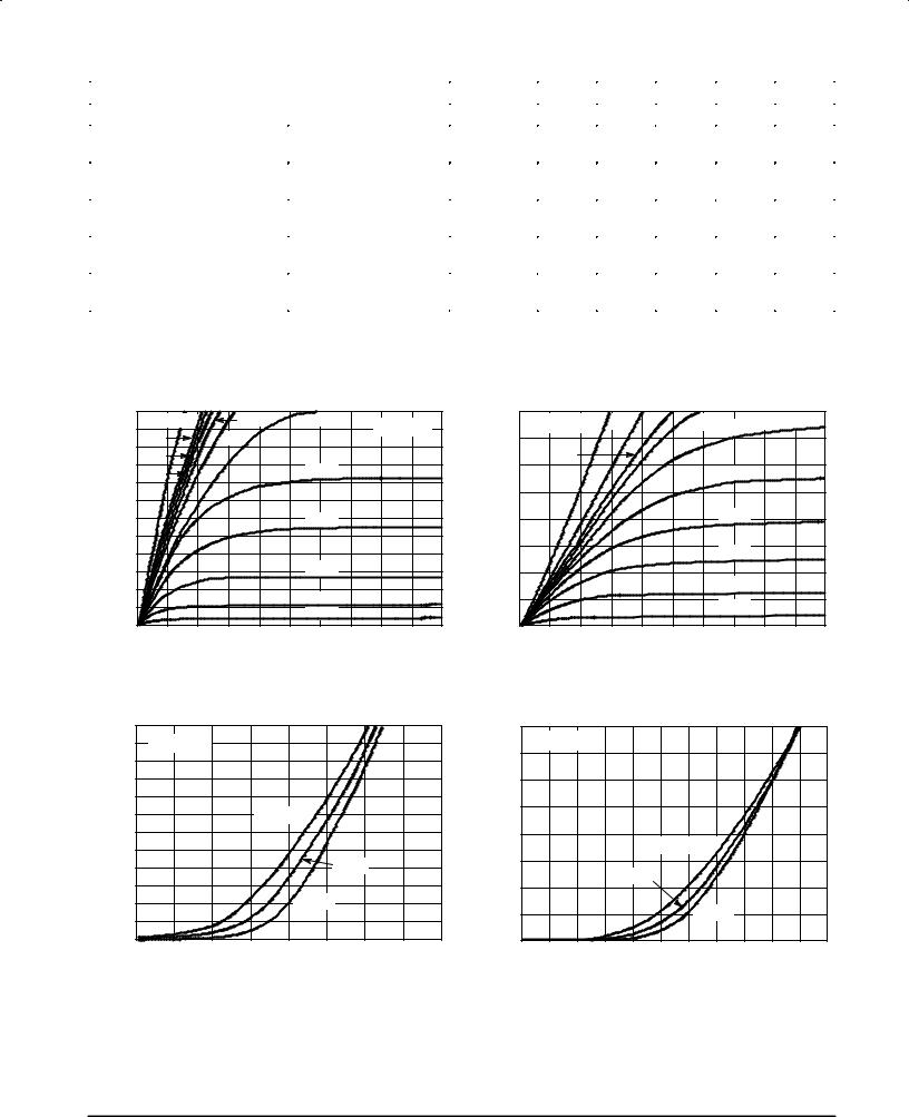
TYPICAL ELECTRICAL CHARACTERISTICS
|
|
|
|
N±Channel |
|
|
|
|
|
|||
|
6 |
VGS = 10 V |
|
3.9 V |
|
3.5 V |
|
TJ = 25°C |
|
4 |
||
|
|
4.5 V |
|
3.7 V |
|
|
|
|
|
|||
(AMPS) |
5 |
|
|
|
|
|
|
(AMPS) |
|
|||
|
4.3 V |
|
|
|
|
|
|
|
|
3 |
||
|
4.1 V |
|
|
|
|
3.3 V |
|
|
|
|||
4 |
|
|
|
|
|
|
|
|
||||
|
|
|
|
|
|
|
|
|
||||
CURRENT |
3 |
|
|
|
|
|
3.1 V |
|
|
|
CURRENT |
2 |
|
|
|
|
|
|
|
|
|
|
|
||
, DRAIN |
2 |
|
|
|
|
|
|
|
|
|
, DRAIN |
|
|
|
|
|
|
|
2.9 V |
|
|
|
1 |
||
D |
|
|
|
|
|
|
|
|
|
D |
||
I |
1 |
|
|
|
|
|
|
|
|
|
I |
|
|
|
|
|
|
|
2.7 V |
|
|
|
|
|
|
|
|
|
|
|
|
|
|
|
|
|
|
|
|
0 |
|
|
|
|
|
2.5 V |
|
|
|
|
0 |
|
0.2 |
0.4 |
0.6 |
0.8 |
1 |
1.2 |
1.4 |
1.6 |
1.8 |
2 |
||
|
0 |
|
||||||||||
|
|
|
|
P±Channel |
|
|
|
|
|
|
|
VGS = 10 V |
4.5 V |
|
3.7 V 3.5 V |
TJ = 25°C |
|
||||
|
3.9 V |
|
|
|
|
|
|
|
|
|
|
|
|
|
|
|
|
3.3 V |
|
|
|
|
|
|
|
|
|
|
3.1 V |
|
|
|
|
|
|
|
|
|
|
2.9 V |
|
|
|
|
|
|
|
|
|
|
2.7 V |
|
|
|
|
|
|
|
|
|
|
2.5 V |
|
|
|
0 |
0.2 |
0.4 |
0.6 |
0.8 |
1 |
1.2 |
1.4 |
1.6 |
1.8 |
2 |
VDS, DRAIN±TO±SOURCE VOLTAGE (VOLTS) |
VDS, DRAIN±TO±SOURCE VOLTAGE (VOLTS) |
Figure 1. On±Region Characteristics |
Figure 1. On±Region Characteristics |
|
6 |
|
|
|
|
|
VDS ≥ |
10 V |
|
|
|
(AMPS) |
5 |
|
|
|
|
4 |
|
|
|
|
|
CURRENT |
|
|
|
|
|
|
|
TJ = 100°C |
|
|
|
3 |
|
|
|
|
|
|
|
|
|
|
|
, DRAIN |
2 |
|
|
25°C |
|
|
|
|
|
|
|
D |
|
|
|
|
|
I |
1 |
|
± 55°C |
|
|
|
|
|
|
||
|
0 |
2.5 |
3 |
3.5 |
4 |
|
2 |
||||
|
|
VGS, GATE±TO±SOURCE VOLTAGE (VOLTS) |
|
||
Figure 2. Transfer Characteristics
|
4 |
VDS ≥ |
10 V |
|
|
|
|
|
|
|
|
|
|
|
|
|
|
|
|
|
|
|
|
||
(AMPS) |
3 |
|
|
|
|
|
|
|
|
|
|
|
|
|
|
|
|
|
|
|
|
|
|
|
|
CURRENT |
2 |
|
|
|
|
TJ = 100°C |
|
|
|
|
||
|
|
|
|
|
|
|
|
|
||||
, DRAIN |
|
|
|
|
|
|
|
|
|
|||
1 |
|
|
|
25°C |
|
|
|
|
|
|
|
|
D |
|
|
|
|
|
|
|
|
|
|
|
|
I |
|
|
|
|
|
|
|
|
|
|
|
|
|
|
|
|
|
|
|
|
± 55°C |
|
|
|
|
|
0 |
1.7 |
1.9 |
2.1 |
2.3 |
2.5 |
2.7 |
2.9 |
3.1 |
3.3 |
3.5 |
3.7 |
|
1.5 |
|||||||||||
|
|
|
VGS, GATE±TO±SOURCE VOLTAGE (VOLTS) |
|
|
|||||||
Figure 2. Transfer Characteristics
Motorola TMOS Power MOSFET Transistor Device Data |
3 |
MMDF2C03HD
TYPICAL ELECTRICAL CHARACTERISTICS
(OHMS) |
|
|
N±Channel |
|
|
|
|
(OHMS) |
||
0.6 |
|
ID = 1.5 A |
|
|
|
|
|
|
||
RESISTANCE |
0.5 |
|
TJ = 25°C |
|
|
|
|
|
|
RESISTANCE |
|
|
|
|
|
|
|
|
|
||
DRAIN±TO±SOURCE, |
0.4 |
|
|
|
|
|
|
|
|
DRAIN±TO±SOURCE, |
0.3 |
|
|
|
|
|
|
|
|
||
|
|
|
|
|
|
|
|
|
|
|
|
0.2 |
|
|
|
|
|
|
|
|
|
DS(on) |
0.1 |
|
|
|
|
|
|
|
|
DS(on) |
0 |
|
|
|
|
|
|
|
|
||
R |
2 |
3 |
4 |
5 |
6 |
7 |
8 |
9 |
10 |
R |
VGS, GATE±TO±SOURCE VOLTAGE (VOLTS)
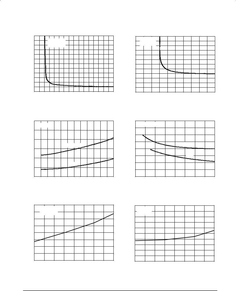
Figure 3. On±Resistance versus
Gate±To±Source Voltage
P±Channel
0.6
ID = 1 A
0.5
TJ = 25°C
0.4
0.3
0.2
0.1
0
0 |
1 |
2 |
3 |
4 |
5 |
6 |
7 |
8 |
9 |
10 |
|
|
VGS, GATE±TO±SOURCE VOLTAGE (VOLTS) |
|
|
||||||
Figure 3. On±Resistance versus
Gate±To±Source Voltage
(OHMS) |
0.08 |
|
|
|
|
|
|
|
|
TJ = 25°C |
|
|
|
|
|
||
RESISTANCE |
0.07 |
|
|
|
|
|
|
|
|
|
|
VGS = 4.5 |
|
|
|
||
, DRAIN±TO±SOURCE |
|
|
|
|
|
|
||
0.06 |
|
|
|
|
|
|
||
|
|
|
10 V |
|
|
|
||
|
|
|
|
|
|
|
||
DS(on) |
0.05 |
|
|
|
|
|
|
|
0 |
0.5 |
1 |
1.5 |
2 |
2.5 |
3 |
||
R |
||||||||
|
|
|
ID, DRAIN CURRENT (AMPS) |
|
|
|||
(OHMS) |
0.30 |
TJ = 25°C |
|
|
|
|
|
|
||
|
|
|
|
|
|
|
||||
RESISTANCE |
0.25 |
|
|
|
|
|
|
|
|
|
|
|
|
|
|
VGS = 4.5 V |
|
|
|
||
, DRAIN±TO±SOURCE |
0.20 |
|
|
|
|
|
|
|
||
|
|
|
|
|
|
|
|
|||
|
|
|
|
|
10 V |
|
|
|
||
0.15 |
|
|
|
|
|
|
|
|
||
|
|
|
|
|
|
|
|
|
||
DS(on) |
0.10 |
|
|
|
|
2.5 |
3 |
3.5 |
|
|
0 |
0.5 |
1 |
1.5 |
2 |
4 |
|||||
R |
||||||||||
|
|
|
|
ID, DRAIN CURRENT (AMPS) |
|
|
|
|||
Figure 4. On±Resistance versus Drain Current |
Figure 4. On±Resistance versus Drain Current |
and Gate Voltage |
and Gate Voltage |
(NORMALIZED) |
2.0 |
VGS = 10 V |
|
|
|
|
|
|
RESISTANCE |
1.6 |
|
|
|
|
|
|
|
|
|
|
|
|
|
|
|
|
|
|
V |
GS |
= 10 V |
|
|
|
|
|
|
|
|||||
|
ID = 1.5 A |
|
|
|
|
|
|
I |
|
= 2 A |
|
|
|
|
|
|
|
||||
|
|
|
|
|
|
|
|
|
D |
|
|
|
|
|
|
|
|
|
|||
1.5 |
|
|
|
|
|
|
|
|
1.4 |
|
|
|
|
|
|
|
|
|
|
||
|
|
|
|
|
|
|
|
|
|
|
|
|
|
|
|
|
|
|
|||
|
|
|
|
|
|
|
|
|
|
|
|
|
|
|
|
|
|
|
|
||
DRAIN±TO±SOURCERESISTANCE |
|
|
|
|
|
|
|
|
|
DRAIN±TO±SOURCE |
1.2 |
|
|
|
|
|
|
|
|
|
|
1.0 |
|
|
|
|
|
|
|
|
|
|
|
|
|
|
|
|
|
|
|
||
|
|
|
|
|
|
|
|
|
1.0 |
|
|
|
|
|
|
|
|
|
|
||
0.5 |
|
|
|
|
|
|
|
|
0.8 |
|
|
|
|
|
|
|
|
|
|
||
|
|
|
|
|
|
|
|
|
, |
|
|
|
|
|
|
|
|
|
|
||
|
|
|
|
|
|
|
|
|
DS(on) (NORMALIZED) |
|
|
|
|
|
|
|
|
|
|
||
|
|
|
|
|
|
|
|
|
|
|
|
|
|
|
|
|
|
|
|
||
, |
0 |
|
|
|
|
|
|
|
|
R |
0.6 |
|
|
|
|
|
|
|
|
|
|
DS(on) |
± 25 |
0 |
25 |
50 |
75 |
100 |
125 |
150 |
|
± 25 |
0 |
25 |
50 |
75 |
100 |
125 |
150 |
||||
± 50 |
± 50 |
|
|||||||||||||||||||
|
|
TJ, JUNCTION TEMPERATURE (°C) |
|
|
|
|
|
|
TJ, JUNCTION TEMPERATURE (°C) |
|
|
||||||||||
R |
|
|
|
|
|
|
|
|
|
|
|
||||||||||
Figure 5. On±Resistance Variation with |
Figure 5. On±Resistance Variation with |
Temperature |
Temperature |
4 |
Motorola TMOS Power MOSFET Transistor Device Data |
MMDF2C03HD
TYPICAL ELECTRICAL CHARACTERISTICS
|
|
|
N±Channel |
|
|
|
|
|
100 |
|
|
|
|
|
|
|
|
VGS = 0 V |
|
|
|
|
|
(nA) |
|
|
|
TJ = 125°C |
|
|
|
|
|
|
|
|
|
|
|
, LEAKAGE |
10 |
|
|
100°C |
|
|
|
|
|
|
|
|
|
|
|
DSS |
|
|
|
|
|
|
|
I |
|
|
|
|
|
|
|
|
1 |
5 |
10 |
15 |
20 |
25 |
30 |
|
0 |
||||||
|
|
VDS, DRAIN±TO±SOURCE VOLTAGE (VOLTS) |
|
||||
|
|
|
P±Channel |
|
|
|
|
|
1000 |
VGS = 0 V |
|
|
|
|
|
|
|
|
|
|
|
|
|
(nA) |
|
|
|
|
|
|
|
, LEAKAGE |
100 |
|
|
TJ = 125°C |
|
|
|
|
|
|
|
|
|
||
|
|
|
|
|
|
|
|
DSS |
|
|
100°C |
|
|
|
|
I |
|
|
|
|
|
|
|
|
|
|
|
|
|
|
|
|
10 |
5 |
10 |
15 |
20 |
25 |
30 |
|
0 |
||||||
|
|
VDS, DRAIN±TO±SOURCE VOLTAGE (VOLTS) |
|
||||
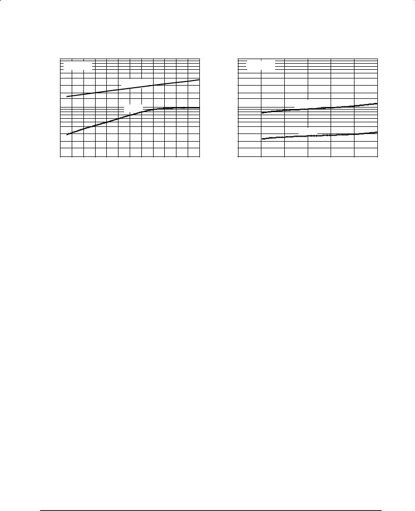
Figure 6. Drain±To±Source Leakage |
Figure 6. Drain±To±Source Leakage |
Current versus Voltage |
Current versus Voltage |
POWER MOSFET SWITCHING
Switching behavior is most easily modeled and predicted by recognizing that the power MOSFET is charge controlled. The lengths of various switching intervals ( t) are determined by how fast the FET input capacitance can be charged by current from the generator.
The published capacitance data is difficult to use for calculating rise and fall because drain±gate capacitance varies greatly with applied voltage. Accordingly, gate charge data is used. In most cases, a satisfactory estimate of average input
current (IG(AV)) can be made from a rudimentary analysis of the drive circuit so that
t = Q/IG(AV)
During the rise and fall time interval when switching a resistive load, VGS remains virtually constant at a level known as the plateau voltage, VSGP. Therefore, rise and fall times may be approximated by the following:
tr = Q2 x RG/(VGG ± VGSP) tf = Q2 x RG/VGSP
where
VGG = the gate drive voltage, which varies from zero to VGG RG = the gate drive resistance
and Q2 and VGSP are read from the gate charge curve.
During the turn±on and turn±off delay times, gate current is not constant. The simplest calculation uses appropriate values from the capacitance curves in a standard equation for voltage change in an RC network. The equations are:
td(on) = RG Ciss In [VGG/(VGG ± VGSP)]
td(off) = RG Ciss In (VGG/VGSP)
The capacitance (Ciss) is read from the capacitance curve at a voltage corresponding to the off±state condition when cal-
culating td(on) and is read at a voltage corresponding to the on±state when calculating td(off).
At high switching speeds, parasitic circuit elements complicate the analysis. The inductance of the MOSFET source lead, inside the package and in the circuit wiring which is common to both the drain and gate current paths, produces a voltage at the source which reduces the gate drive current. The voltage is determined by Ldi/dt, but since di/dt is a function of drain current, the mathematical solution is complex. The MOSFET output capacitance also complicates the mathematics. And finally, MOSFETs have finite internal gate resistance which effectively adds to the resistance of the driving source, but the internal resistance is difficult to measure and, consequently, is not specified.
The resistive switching time variation versus gate resistance (Figure 9) shows how typical switching performance is affected by the parasitic circuit elements. If the parasitics were not present, the slope of the curves would maintain a value of unity regardless of the switching speed. The circuit used to obtain the data is constructed to minimize common inductance in the drain and gate circuit loops and is believed readily achievable with board mounted components. Most power electronic loads are inductive; the data in the figure is taken with a resistive load, which approximates an optimally snubbed inductive load. Power MOSFETs may be safely operated into an inductive load; however, snubbing reduces switching losses.
Motorola TMOS Power MOSFET Transistor Device Data |
5 |