Материал: 271024
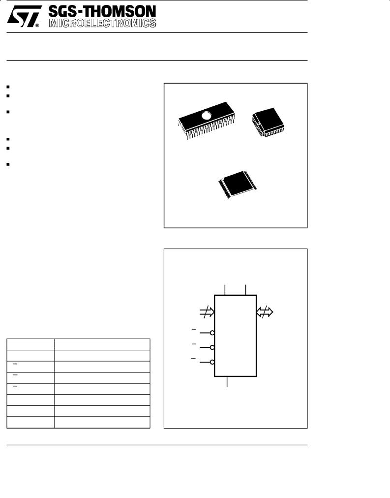
M27C1024
1 Megabit (64K x16) UV EPROM and OTP ROM
VERY FAST ACCESS TIME: 55ns
COMPATIBLE with HIGH SPEED MICROPROCESSORS, ZERO WAIT STATE
LOW POWER ºCMOSº CONSUMPTION:
± Active Current 35mA
± Standby Current 100μA |
40 |
|
|
|
|
||
PROGRAMMING VOLTAGE: 12.75V |
1 |
|
|
ELECTRONIC SIGNATURE for AUTOMATED |
FDIP40W (F) |
PLCC44 (C) |
|
PROGRAMMING |
|||
|
|
PROGRAMMING TIME of AROUND 6 sec. (PRESTO II ALGORITHM)
DESCRIPTION
The M27C1024 is a 1 Megabit UV erasable and electrically programmable read only memory (EPROM). It is organized as 65,536 words by 16 bits.
The 40 pin Ceramic Frit Seal Window package has a transparent lid which allows the user to expose the chip to ultraviolet light to erase the bit pattern. A new pattern can then be written to the device by following the programming procedure.
For application where the content is programmed only one time and erasure is not required, the M27C1024 is offered in a Plastic Leaded Chip Carrier package.
Table 1. Signal Names
A0 - A15 |
Address Inputs |
Q0 - Q15 |
Data Outputs |
E |
Chip Enable |
G |
Output Enable |
P |
Program |
VPP |
Program Supply |
VCC |
Supply Voltage |
VSS |
Ground |
TSOP40 (N) 10 x 14mm
Figure 1. Logic Diagram
VCC |
VPP |
16 |
16 |
A0-A15 |
Q0-Q15 |
P M27C1024
E
G
VSS
AI00702B
March 1996 |
1/13 |
M27C1024
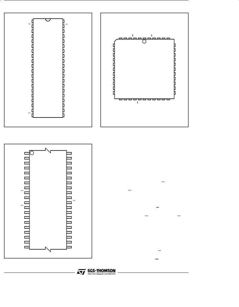
Figure 2A. DIP Pin Connections
VPP |
1 |
|
40 |
VCC |
E |
2 |
|
39 |
P |
Q15 |
3 |
|
38 |
NC |
Q14 |
4 |
|
37 |
A15 |
Q13 |
5 |
|
36 |
A14 |
Q12 |
6 |
|
35 |
A13 |
Q11 |
7 |
|
34 |
A12 |
Q10 |
8 |
|
33 |
A11 |
Q9 |
9 |
|
32 |
A10 |
Q8 |
10 |
M27C1024 |
31 |
A9 |
VSS |
11 |
30 |
VSS |
|
Q7 |
12 |
|
29 |
A8 |
Q6 |
13 |
|
28 |
A7 |
Q5 |
14 |
|
27 |
A6 |
Q4 |
15 |
|
26 |
A5 |
Q3 |
16 |
|
25 |
A4 |
Q2 |
17 |
|
24 |
A3 |
Q1 |
18 |
|
23 |
A2 |
Q0 |
19 |
|
22 |
A1 |
G |
20 |
|
21 |
A0 |
|
|
AI00703 |
|
|
Warning: NC = Not Connected.
Figure 2C. TSOP Pin Connections
A9 |
1 |
|
40 |
VSS |
A10 |
|
|
|
A8 |
A11 |
|
|
|
A7 |
A12 |
|
|
|
A6 |
A13 |
|
|
|
A5 |
A14 |
|
|
|
A4 |
A15 |
|
|
|
A3 |
NC |
|
|
|
A2 |
P |
|
|
|
A1 |
VCC |
10 |
M27C1024 |
31 |
A0 |
VPP |
11 |
(Normal) |
30 |
G |
E |
|
|
|
DQ0 |
DQ15 |
|
|
|
DQ1 |
DQ14 |
|
|
|
DQ2 |
DQ13 |
|
|
|
DQ3 |
DQ12 |
|
|
|
DQ4 |
DQ11 |
|
|
|
DQ5 |
DQ10 |
|
|
|
DQ6 |
DQ9 |
|
|
|
DQ7 |
DQ8 |
20 |
|
21 |
VSS |
|
|
|
AI01582 |
|
Warning: NC = Not Connected.
Figure 2B. LCC Pin Connections
Q13 |
Q14 |
Q15 |
E |
PP |
NC |
CC |
P |
NC |
A15 |
A14 |
V |
V |
|||||||||
Q12 |
|
|
|
|
1 |
44 |
|
|
|
A13 |
|
|
|
|
|
|
|
|
|
||
Q11 |
|
|
|
|
|
|
|
|
|
A12 |
Q10 |
|
|
|
|
|
|
|
|
|
A11 |
Q9 |
|
|
|
|
|
|
|
|
|
A10 |
Q8 |
|
|
|
|
|
|
|
|
|
A9 |
VSS 12 |
|
|
|
M27C1024 |
|
|
|
34 VSS |
||
NC |
|
|
|
|
|
|
|
|
|
NC |
Q7 |
|
|
|
|
|
|
|
|
|
A8 |
Q6 |
|
|
|
|
|
|
|
|
|
A7 |
Q5 |
|
|
|
|
|
|
|
|
|
A6 |
Q4 |
|
|
|
|
23 |
|
|
|
|
A5 |
|
|
|
|
|
|
|
|
|
|
|
Q3 |
Q2 |
Q1 |
Q0 |
G |
NC |
A0 |
A1 A2 |
A3 |
A4 |
|
|
|
|
|
|
|
|
|
|
|
AI00704 |
Warning: NC = Not Connected.
DEVICE OPERATION
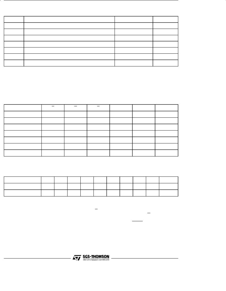
The modes of operations of the M27C1024 are listed in the Operating Modes table. A single 5V power supply is required in the read mode. All inputs are TTL levels except for Vpp and 12V on A9 for Electronic Signature.
Read Mode
The M27C1024 has two control functions, both of which must be logically active in order to obtain data at the outputs. Chip Enable (E) is the power control and should be used for device selection. Output Enable (G) is the output control and should be used to gate data to the output pins, independent of device selection. Assuming that the addresses are stable, the address access time
(tAVQV) is equal to the delay from E to output (tELQV). Data is available at the output after a delay of tOE
from the falling edge of G, assuming that E has been low and the addresses have been stable for at least tAVQV-tGLQV.
Standby Mode
The M27C1024 has a standby mode which reduces the active current from 35mA to 100μA.
The M27C1024 is placed in the standby mode by applying a TTL high signal to the E input. When in the standbymode, the outputs are in a high impedance state, independent of the G input.
2/13
|
|
|
M27C1024 |
Table 2. Absolute Maximum Ratings (1) |
|
|
|
Symbol |
Parameter |
Value |
Unit |
TA |
Ambient Operating Temperature |
±40 to 125 |
°C |
TBIAS |
Temperature Under Bias |
±50 to 125 |
°C |
TSTG |
Storage Temperature |
±65 to 150 |
°C |
VIO (2) |
Input or Output Voltages (except A9) |
±2 to 7 |
V |
VCC |
Supply Voltage |
±2 to 7 |
V |
(2) |
A9 Voltage |
±2 to 13.5 |
V |
VA9 |
|||
VPP |
Program Supply Voltage |
±2 to 14 |
V |
Notes: 1. Except for the rating ºOperating Temperature Rangeº, stresses above those listed in the Table ºAbsolute Maximum Ratingsº may cause permanent damage to the device. These are stress ratings only and operation of the device at these or any other conditions above those indicated in the Operating sections of this specification is not implied. Exposure to Absolute Maximum Rating conditions for extended periods may affect device reliability. Refer also to the SGS-THOMSON SURE Program and other relevant quality documents.
2.Minimum DC voltage on Input or Output is ±0.5V with possible undershoot to ±2.0V for a period less than 20ns. Maximum DC voltage on Output is VCC +0.5V with possible overshoot to VCC +2V for a period less than 20ns.
Table 3. Operating Modes
Mode |
E |
G |
P |
A9 |
VPP |
Q0 - Q15 |
Read |
VIL |
VIL |
VIH |
X |
VCC or VSS |
Data Output |
Output Disable |
VIL |
VIH |
X |
X |
VCC or VSS |
Hi-Z |
Program |
VIL |
X |
VIL Pulse |
X |
VPP |
Data Input |
Verify |
VIL |
VIL |
VIH |
X |
VPP |
Data Output |
Program Inhibit |
VIH |
X |
X |
X |
VPP |
Hi-Z |
Standby |
VIH |
X |
X |
X |
VCC or VSS |
Hi-Z |
Electronic Signature |
VIL |
VIL |
VIH |
VID |
VCC |
Codes |
Note: X = VIH or VIL, VID = 12V ±0.5V |
|
|
|
|
|
|
Table 4. Electronic Signature
Identifier |
A0 |
Q7 |
Q6 |
Q5 |
Q4 |
Q3 |
Q2 |
Q1 |
Q0 |
Hex Data |
Manufacturer's Code |
VIL |
0 |
0 |
1 |
0 |
0 |
0 |
0 |
0 |
20h |
Device Code |
VIH |
1 |
0 |
0 |
0 |
1 |
1 |
0 |
0 |
8Ch |
Two Line Output Control
Because EPROMs are usually used in larger memory arrays, this product features a 2 line control function which accommodates the use of multiple memory connection. The two line control function allows:
a.the lowest possible memory power dissipation,
b.complete assurance that output bus contention will not occur.
For the most efficient use of these two control lines, E should be decoded and used as the primary device selecting function, while G should be made a common connection to all devices in the array and connected to the READ line from the system control bus. This ensures that all deselected memory devices are in their low power standby mode and that the output pins are only active when data is required from a particular memory device.
3/13
M27C1024
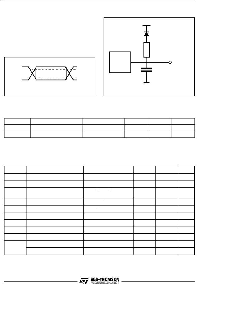
AC MEASUREMENT CONDITIONS
Input Rise and Fall Times |
≤ 20ns |
Input Pulse Voltages |
0.4V to 2.4V |
Input and Output Timing Ref. Voltages |
0.8V to 2.0V |
Note that Output Hi-Z is defined as the point where data is no longer driven.
Figure 3. AC Testing Input Output Waveforms
2.4V
2.0V
0.8V
0.4V
AI00826
Figure 4. AC Testing Load Circuit
1.3V
1N914
3.3kΩ
DEVICE
UNDER OUT TEST
CL = 100pF
CL includes JIG capacitance
AI00828
Note: For 55ns class: input pulse voltages are 0V to 3V, input output test points are at 1.5V, CL is 30 pF.
Table 5. Capacitance (1) (TA = 25 °C, f = 1 MHz )
Symbol |
Parameter |
Test Condition |
Min |
Max |
Unit |
CIN |
Input Capacitance |
VIN = 0V |
|
6 |
pF |
COUT |
Output Capacitance |
VOUT = 0V |
|
12 |
pF |
Note: 1. Sampled only, not 100% tested.
Table 6. Read Mode DC Characteristics (1)
(TA = 0 to 70 °C, ±40 to 85 °C or ±40 to 105 °C; VCC = 5V ± 5% or 5V ± 10%; VPP = VCC)
Symbol |
Parameter |
Test Condition |
Min |
Max |
Unit |
ILI |
Input Leakage Current |
0V ≤ VIN ≤ VCC |
|
±10 |
μA |
ILO |
Output Leakage Current |
0V ≤ VOUT ≤ VCC |
|
±10 |
μA |
ICC |
Supply Current |
E = VIL, G = VIL, |
|
35 |
mA |
IOUT = 0mA, f = 5MHz |
|
||||
|
|
|
|
|
|
ICC1 |
Supply Current (Standby) TTL |
E = VIH |
|
1 |
mA |
ICC2 |
Supply Current (Standby) CMOS |
E > VCC ± 0.2V |
|
100 |
μA |
IPP |
Program Current |
VPP = VCC |
|
100 |
μA |
VIL |
Input Low Voltage |
|
±0.3 |
0.8 |
V |
(2) |
Input High Voltage |
|
2 |
VCC + 1 |
V |
VIH |
|
||||
VOL |
Output Low Voltage |
IOL = 2.1mA |
|
0.4 |
V |
VOH |
Output High Voltage TTL |
IOH = ±400μA |
2.4 |
|
V |
|
IOH = ±100μA |
|
|
|
|
|
Output High Voltage CMOS |
VCC ± 0.7V |
|
V |
Notes: 1. VCC must be applied simultaneously with or before VPP and removed simultaneously with or after VPP. 2. Maximum DC voltage on Output is VCC +0.5V.
4/13
M27C1024
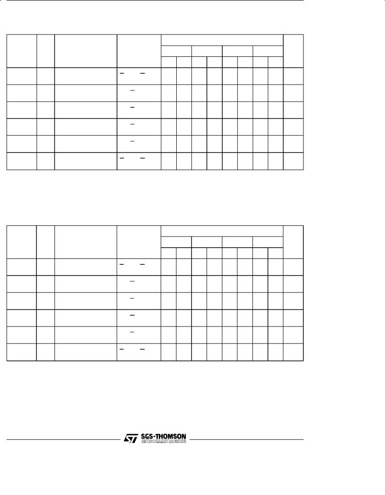
Table 7A. Read Mode AC Characteristics (1)
(TA = 0 to 70 °C, ±40 to 85 °C or ±40 to 105 °C; VCC = 5V ± 5% or 5V ± 10%; VPP = VCC)
|
|
|
|
|
|
|
M27C1024 |
|
|
|
|
|
Symbol |
Alt |
Parameter |
Test Condition |
-55 (3) |
-70 |
-80 |
-90 |
Unit |
||||
|
|
|
|
Min |
Max |
Min |
Max |
Min |
Max |
Min |
Max |
|
tAVQV |
tACC |
Address Valid to |
E = VIL, G = VIL |
|
55 |
|
70 |
|
80 |
|
90 |
ns |
Output Valid |
|
|
|
|
||||||||
|
|
|
|
|
|
|
|
|
|
|
|
|
tELQV |
tCE |
Chip Enable Low to |
G = VIL |
|
55 |
|
70 |
|
80 |
|
90 |
ns |
Output Valid |
|
|
|
|
||||||||
|
|
|
|
|
|
|
|
|
|
|
|
|
tGLQV |
tOE |
Output Enable Low to |
E = VIL |
|
30 |
|
35 |
|
40 |
|
45 |
ns |
Output Valid |
|
|
|
|
||||||||
|
|
|
|
|
|
|
|
|
|
|
|
|
(2) |
tDF |
Chip Enable High to |
G = VIL |
0 |
30 |
0 |
30 |
0 |
30 |
0 |
30 |
ns |
tEHQZ |
Output Hi-Z |
|||||||||||
|
|
|
|
|
|
|
|
|
|
|
|
|
(2) |
tDF |
Output Enable High to |
E = VIL |
0 |
30 |
0 |
30 |
0 |
30 |
0 |
30 |
ns |
tGHQZ |
Output Hi-Z |
|||||||||||
|
|
|
|
|
|
|
|
|
|
|
|
|
tAXQX |
tOH |
Address Transition to |
E = VIL, G = VIL |
0 |
|
0 |
|
0 |
|
0 |
|
ns |
Output Transition |
|
|
|
|
||||||||
|
|
|
|
|
|
|
|
|
|
|
|
|
Notes: 1. VCC must be applied simultaneously with or before VPP and removed simultaneously with or after VPP.
2.Sampled only, not 100% tested.
3.See specific AC Measurement Condition for -55 class.
Table 7B. Read Mode AC Characteristics (1)
(TA = 0 to 70 °C, ±40 to 85 °C or ±40 to 105 °C; VCC = 5V ± 5% or 5V ± 10%; VPP = VCC)
|
|
|
|
|
|
|
M27C1024 |
|
|
|
||
Symbol |
Alt |
Parameter |
Test Condition |
-10 |
|
-12 |
|
-15 |
-20/-25 |
Unit |
||
|
|
|
|
|
|
|
||||||
|
|
|
|
Min |
Max Min Max Min Max Min Max |
|
||||||
tAVQV |
tACC |
Address Valid to |
E = VIL, G = VIL |
|
100 |
|
120 |
|
150 |
|
200 |
ns |
Output Valid |
|
|
|
|
||||||||
|
|
|
|
|
|
|
|
|
|
|
|
|
tELQV |
tCE |
Chip Enable Low to |
G = VIL |
|
100 |
|
120 |
|
150 |
|
200 |
ns |
Output Valid |
|
|
|
|
||||||||
|
|
|
|
|
|
|
|
|
|
|
|
|
tGLQV |
tOE |
Output Enable Low to |
E = VIL |
|
50 |
|
60 |
|
60 |
|
70 |
ns |
Output Valid |
|
|
|
|
||||||||
|
|
|
|
|
|
|
|
|
|
|
|
|
(2) |
tDF |
Chip Enable High to |
G = VIL |
0 |
30 |
0 |
40 |
0 |
50 |
0 |
60 |
ns |
tEHQZ |
Output Hi-Z |
|||||||||||
|
|
|
|
|
|
|
|
|
|
|
|
|
(2) |
tDF |
Output Enable High to |
E = VIL |
0 |
30 |
0 |
40 |
0 |
50 |
0 |
60 |
ns |
tGHQZ |
Output Hi-Z |
|||||||||||
|
|
|
|
|
|
|
|
|
|
|
|
|
tAXQX |
tOH |
Address Transition to |
E = VIL, G = VIL |
0 |
|
0 |
|
0 |
|
0 |
|
ns |
Output Transition |
|
|
|
|
||||||||
|
|
|
|
|
|
|
|
|
|
|
|
|
Notes: 1. VCC must be applied simultaneously with or before VPP and removed simultaneously with or after VPP. 2. Sampled only, not 100% tested.
5/13